60
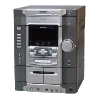
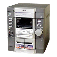
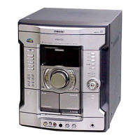
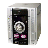
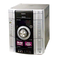
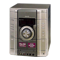
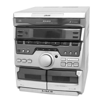
HCD-RV7/RV8
Pin No. Pin Name I/O Description
203 AUDBCK O
Serial audio bit clock signal (2.8224 MHz) output to the digital filter
204 AUDLRCK O
Serial audio L/R sampling clock signal (44.1 kHz) output to the digital filter
205 AUDXCLKO O
Serial audio clock signal output to the digital filter
206 CLKA I
Sub system clock input terminal (27 MHz)
207 CLKB O
Sub system clock output terminal (27 MHz)
208 VDD9 —
Digital power supply terminal (+2.5V) (for CD-DSP block)
209 THRCLK I
Clock signal input terminal for the test Not used
210 TESTEN I
Setting terminal for the test Normally: fixed at “L”
211 TCLK I
Clock signal input terminal for the test Not used
212 TMODE1 I
Selection signal input terminal for the test Not used
213 TRST I
Reset signal input terminal for the test Not used
214 VSS9 —
Digital ground terminal
215 V AVS1 —
Analog ground terminal (for D/A converter)
216 V AVD1 —
Analog power supply terminal (+2.5V) (for D/A converter)
w
w
w
.
x
i
a
o
y
u
1
6
3
.
c
o
m
Q
Q
3
7
6
3
1
5
1
5
0
9
9
2
8
9
4
2
9
8
T
E
L
1
3
9
4
2
2
9
6
5
1
3
9
9
2
8
9
4
2
9
8
0
5
1
5
1
3
6
7
3
Q
Q
TEL 13942296513 QQ 376315150 892498299
TEL 13942296513 QQ 376315150 892498299
http://www.xiaoyu163.com
http://www.xiaoyu163.com