EasyManua.ls Logo

Sony HCD-RV6 - User Manual

Sony HCD-RV6
106 pages
Print Icon
To Next Page IconTo Next Page
Loading...
1
Ver 1.4 2004. 04
Model Name Using Similar Mechanism NEW
CD CD Mechanism Type CDM58E-30BD62
Section Base Unit Name BU-30BD62
Optical Pick-up Name A-MAX.3
Tape Deck
Model Name Using Similar Machanism NEW
Section Tape Transport Mechanism Type
RV2: CWM43FF-05
RV5/RV6: CWM48RR-01
SERVICE MANUAL
E Model
HCD-RV2/RV5/RV6
Tourist Model
HCD-RV5
HCD-RV2/RV5/RV6
Amplifier section
HCD-RV2:
The following measured at AC 120, 127, 220, 240 V,
50/60 Hz
DIN power output (rated)
50 + 50 watts
Continuous RMS power output (reference)
60 + 60 watts (6 ohms at
1 kHz, 10% THD)
HCD-RV6:
The following measured at AC 120, 127, 220, 240 V,
50/60 Hz
DIN power output (rated)
115 + 115 watts
Continuous RMS power output (reference)
140 + 140 watts (6 ohms at
1 kHz, 10% THD)
HCD-RV5:
The following measured at AC 120, 127, 220, 240 V,
50/60 Hz
DIN power output (rated)
100 + 100 watts
Continuous RMS power output (reference)
120 + 120 watts (6 ohms at
1 kHz, 10% THD)
SPECIFICATIONS
Inputs
HCD-RV2:
GAME INPUT (VIDEO) (phono jack):
1 Vp-p, 75 ohms
GAME INPUT (AUDIO) (phono jacks):
voltage 450 mV,
impedance 47 kilohms
MIC (phone jack): sensitivity 1 mV,
impedance 10 kilohms
Outputs
VIDEO OUT (phono jack):
max. output level
1 Vp-p, unbalanced, Sync
negative, load impedance
75 ohms
PHONES (stereo mini jack):
accepts headphones of
8 ohms or more
SPEAKER: accepts impedance of 6 to
16 ohms
Sony Corporation
Home Audio Company
Published by Sony Engineering Corporation
9-874-131-05
2004D04-1
© 2004. 04
– Continued on next page –
COMPACT DISC DECK RECEIVER
• HCD-RV2/RV5/RV6 are the tuner,
deck, CD and amplifier section in
MHC-RV2/RV5/RV6.
w
w
w
.
x
i
a
o
y
u
1
6
3
.
c
o
m
Q
Q
3
7
6
3
1
5
1
5
0
9
9
2
8
9
4
2
9
8
T
E
L
1
3
9
4
2
2
9
6
5
1
3
9
9
2
8
9
4
2
9
8
0
5
1
5
1
3
6
7
3
Q
Q
TEL 13942296513 QQ 376315150 892498299
http://www.xiaoyu163.com

Table of Contents

Question and Answer IconNeed help?

Do you have a question about the Sony HCD-RV6 and is the answer not in the manual?

Sony HCD-RV6 Specifications

General IconGeneral
BrandSony
ModelHCD-RV6
CategoryStereo System
LanguageEnglish

Summary

Service Manual Overview

Specifications Summary

Technical specifications including inputs, outputs, and impedance for different models.

General Information and Specifications

Speaker and Player Specifications

Details on speaker systems, disc player, tape deck, and tuner specifications.

Important Notes and Precautions

Handling Optical Pick-up and Laser Diode

Precautions for handling optical pick-up, laser diode emission checks, and component replacement.

Circuit Board Repair and Model Identification

Guidelines for flexible circuit board repair, soldering, and model identification.

CD Disc Tray Lock Function

Procedure for setting and releasing the CD disc tray lock function for security.

SECTION 1 SERVICE NOTE

Panel and Key Board Removal;Installation

Instructions for removing and installing the panel and key boards, including screw usage.

SECTION 2 GENERAL

Main Unit and Remote Control Overview (HCD-RV2)

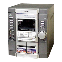
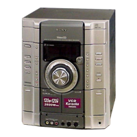
Diagrams and control descriptions for the HCD-RV2 main unit and remote control.

Main Unit and Remote Control Overview (HCD-RV5;RV6)

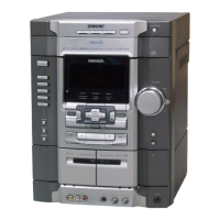
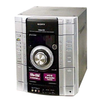
Diagrams and control descriptions for the HCD-RV5/RV6 main unit and remote control.

SECTION 3 DISASSEMBLY

Disassembly Steps Overview

Flowchart outlining the sequence for disassembling the unit, from case to component boards.

3-3. CD (DOOR) Disassembly

Diagram and procedure for removing the CD door and mechanism.

3-4. FRONT PANEL SECTION Disassembly

Diagram and procedure for disassembling the front panel section.

3-5. TAPE MECHANISM DECK Disassembly

Diagram and procedure for disassembling the tape mechanism deck.

3-6. PANEL BOARD Disassembly

Diagram and procedure for disassembling the panel board.

3-7. KEY BOARD Disassembly

Diagram and procedure for disassembling the key board.

3-8. SENSOR BOARD, DC FAN Disassembly

Diagram and procedure for disassembling the sensor board and DC fan.

3-9. MAIN BOARD, POWER AMP BOARD Disassembly

Diagram and procedure for disassembling the main and power amp boards.

3-10. BASE UNIT Disassembly

Diagram and procedure for disassembling the base unit.

3-11. DRIVER BOARD, MOTOR BOARD, SENSOR (CD) BOARD Disassembly

Diagram and procedure for disassembling driver, motor, and sensor (CD) boards.

SECTION 4 DIAGRAMS

Circuit Boards Location

Diagram showing the location of various circuit boards within the main unit.

BD Board Waveforms

Waveforms for the BD board, including IC103 and its related signals.

VIDEO Board Waveforms

Waveforms for the VIDEO board, including IC505 signals.

MAIN Board Waveforms

Waveforms for the MAIN board, including IC102 and IC601 signals.

PANEL Board Waveforms

Waveforms for the PANEL board, including IC701 signals.

4-2. PRINTED WIRING BOARD - BD SECTION -

4-3. SCHEMATIC DIAGRAM - BD SECTION -

4-4. PRINTED WIRING BOARDS - CD SECTION -

4-5. SCHEMATIC DIAGRAM - CD SECTION -

4-6. PRINTED WIRING BOARD - VIDEO SECTION -

4-7. SCHEMATIC DIAGRAM - VIDEO SECTION (1;2) -

4-8. SCHEMATIC DIAGRAM - VIDEO SECTION (2;2) -

4-9. SCHEMATIC DIAGRAM - MAIN SECTION (1;4) -

4-10. SCHEMATIC DIAGRAM - MAIN SECTION (2;4) -

4-11. SCHEMATIC DIAGRAM - MAIN SECTION (3;4) -

4-12. SCHEMATIC DIAGRAM - MAIN SECTION (4;4) -

4-13. PRINTED WIRING BOARDS - MAIN SECTION -

4-14. PRINTED WIRING BOARDS - PANEL SECTION (HCD-RV2) -

4-15. PRINTED WIRING BOARD - KEY SECTION (HCD-RV2) -

4-16. SCHEMATIC DIAGRAM - PANEL SECTION (HCD-RV2) -

4-17. PRINTED WIRING BOARDS - PANEL SECTION (HCD-RV5) -

4-18. PRINTED WIRING BOARD - KEY SECTION (HCD-RV5) -

4-19. SCHEMATIC DIAGRAM - PANEL SECTION (HCD-RV5) -

4-20. PRINTED WIRING BOARDS - PANEL SECTION (HCD-RV6) -

4-21. PRINTED WIRING BOARD - KEY SECTION (HCD-RV6) -

4-22. SCHEMATIC DIAGRAM - PANEL SECTION (HCD-RV6) -

4-23. PRINTED WIRING BOARD - POWER AMP SECTION (HCD-RV2) -

4-24. PRINTED WIRING BOARD - TRANS SECTION (HCD-RV2) -

4-25. PRINTED WIRING BOARD - SUB TRANS SECTION (HCD-RV2) -

4-26. SCHEMATIC DIAGRAM - POWER SECTION (HCD-RV2) -

4-27. PRINTED WIRING BOARDS - POWER AMP SECTION (HCD-RV5) -

4-28. PRINTED WIRING BOARD - TRANS SECTION (HCD-RV5) -

4-29. PRINTED WIRING BOARD - SUB TRANS SECTION (HCD-RV5) -

4-30. SCHEMATIC DIAGRAM - POWER SECTION (HCD-RV5) -

4-31. PRINTED WIRING BOARDS - POWER AMP SECTION (HCD-RV6) -

4-32. PRINTED WIRING BOARD - TRANS SECTION (HCD-RV6) -

4-33. PRINTED WIRING BOARD - SUB TRANS SECTION (HCD-RV6) -

4-34. SCHEMATIC DIAGRAM - POWER SECTION (HCD-RV6) -

4-35. IC BLOCK DIAGRAMS

IC102 AN41020 A (BD BOARD) Pin Description

Block diagram and pin description for IC102 on the BD board.

IC103 CXA2581 N-T4 (BD BOARD) Pin Description

Block diagram and pin description for IC103 on the BD board.

IC301 BA7046 F-E2 (VIDEO BOARD) Pin Description

Block diagram and pin description for IC301 on the VIDEO board.

IC303 NJM2255 M (TE2) (VIDEO BOARD) Pin Description

Block diagram and pin description for IC303 on the VIDEO board.

IC701 BA6956 AN (DRIVER BOARD) Pin Description

Block diagram and pin description for IC701 on the DRIVER board.

IC304 NJM2209 M (TE2) (VIDEO BOARD) Pin Description

Block diagram and pin description for IC304 on the VIDEO board.

IC504 PCM1748 E;2 K (VIDEO BOARD) Block Diagram

Block diagram for IC504, detailing its functions and pins.

IC506 BU2507 FV-E2 (VIDEO BOARD) Block Diagram

Block diagram for IC506, detailing its functions and pins.

IC101 LA1845 (MAIN BOARD) Block Diagram

Block diagram for IC101, detailing its AM/FM radio functions.

IC301 M61519 FPD61 G (MAIN BOARD) Block Diagram

Block diagram for IC301, detailing its audio processing functions.

IC304 LA2615 (MAIN BOARD) Block Diagram

Block diagram for IC304, detailing its analog surround functions.

IC703 M65850 FP (PANEL BOARD) Block Diagram

Block diagram for IC703, detailing its main control functions.

IC704 NJM2244 M-TE2 (PANEL BOARD) Block Diagram

Block diagram for IC704, detailing its bias and output functions.

SECTION 5 EXPLODED VIEWS

5-1. MAIN SECTION Exploded View

Exploded view of the main section, showing components like the main board and power transformer.

5-2. FRONT PANEL SECTION Exploded View

Exploded view of the front panel section, detailing knobs, display, and buttons.

5-3. MAIN BOARD SECTION Exploded View

Exploded view of the main board section, showing the main board, power amp board, and transformer.

5-4. CD MECHANISM DECK SECTION Exploded View

Exploded view of the CD mechanism deck, detailing its parts like motor, driver board, and sensors.

5-5. BASE UNIT SECTION Exploded View

Exploded view of the base unit section, showing the BD board and optical pick-up assembly.

SECTION 6 ELECTRICAL PARTS LIST

Capacitors, Connectors, ICs, Transistors, Resistors

List of capacitors, connectors, ICs, transistors, and resistors with part numbers and specifications.

Diodes and Switches List

List of diodes and switches used in the unit, including part numbers and functions.

Filters and Other Components List

List of filters and other miscellaneous components used in the unit.

1. TEST MODE

Cold and Hot Reset Procedures

Procedures for performing cold and hot resets to restore factory default settings.

Tuner Step and Function Change Modes

Modes for changing tuner step and switching between VIDEO/MD functions.

GC Test Mode Overview

Test mode for checking controls, including key, count, headphone, and volume checks.

2. MECHANICAL ADJUSTMENTS

Precautions and Torque Measurements

Precautions for cleaning, demagnetizing, and handling parts during mechanical adjustments.

CD Service and Ship Modes

CD Service Mode and Error History

Procedure for CD service mode and explanation of error history display codes.

CD Ship Modes (Memory Clear;No Memory)

Modes for preparing the CD pickup for shipping, with or without memory clear.

3. ELECTRICAL ADJUSTMENTS

Tape Deck Adjustments

Procedures for demagnetizing heads and adjusting azimuth for tape decks.

Output Peak Adjustment

Procedure for adjusting output peaks for L-CH and R-CH signals.

TUNER SECTION Adjustments

FM Tuned Level and Null Adjustment

Procedures for FM tuned level adjustment and null adjustment of the tuner section.

CD SECTION Checks

S-Curve, RF Level, and Traverse Level Checks

Procedures for performing S-curve, RF level, and traverse level checks on the CD player.

VIDEO SECTION Adjustments

Video Level and Audio Checks

Procedure for adjusting video level and checking audio level, clock, and servo signals.

4. IC PIN FUNCTION DESCRIPTION

IC601 (System Control) Pin Description

Pin description for IC601, the system control IC on the main board.

IC701 (Display Control HCD-RV2) Pin Description

Pin description for IC701, the display control IC on the HCD-RV2 panel board.

IC701 (Display Control HCD-RV5;RV6) Pin Description

Pin description for IC701, the display control IC on the HCD-RV5/RV6 panel board.

5. BLOCK DIAGRAM - CD, VIDEO SECTION -

6. BLOCK DIAGRAM - TUNER, POWER SECTION -

7. BLOCK DIAGRAM - MAIN SECTION (HCD-RV2) -

8. BLOCK DIAGRAM - MAIN SECTION (HCD-RV5) -

9. BLOCK DIAGRAM - MAIN SECTION (HCD-RV6) -

REVISION HISTORY

Related product manuals