Do you have a question about the Sony HCD-RG22 and is the answer not in the manual?
Details power output and distortion for various models.
Lists system, laser, frequency response, and SNR.
Describes recording system and frequency response.
Details FM/AM tuning ranges and IF.
Specifies AC leakage limits and measurement methods.
Guidelines for optical pick-up, laser diode, and emission checks.
Notes on chip replacement and flexible circuit board repair.
General caution and critical component warnings.
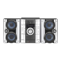
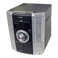
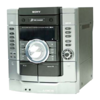
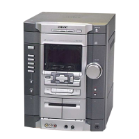
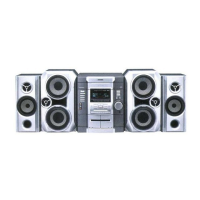
Details main unit components and button functions.
Step-by-step instructions for setting the system clock.
Procedure for disassembling the top case.
Procedure for removing the CD door.
Steps to disassemble the front panel.
Steps to remove the CD mechanism deck.
Steps to remove the tape mechanism deck.
Procedure for removing REM and PANEL boards.
Steps to remove the KEY board.
Procedure for removing the back panel.
Steps to remove Sub Trans, Video Out, and Sensor boards.
Steps to remove MAIN and POWER boards.
Steps to remove TRANS and CD/DRIVER boards.
Steps to remove SPDL board and Optical Pick-up.
Steps to remove MOTOR/SENSOR boards and Cam/Motor.
Switch AM tuner steps between 9 kHz and 10 kHz.
Clears preset data to initial conditions.
Checks CD and tape deck operation, including error displays.
Includes GC, MC, Version, CD Service, and CD Ship modes.
Adjust AM IF for maximum level meter reading.
Adjust FM tuned level for TUNED indicator.
Adjust T101 for 0V between specific pins.
Checks RF signal level and waveform clarity.
Illustrates physical placement of circuit boards.
Shows functional blocks and interconnections for the CD system.
Illustrates functional blocks and interconnections of the main unit.
Shows component layout for the CD section's PWB.
Shows component layout for the second part of CD section's PWB.
Shows component layout for the MAIN board's PWB.
Shows component layout for the PANEL section's PWBs.
Shows component layouts for POWER and TRANS boards.
Provides the detailed circuit schematic for the CD section.
First part of the circuit schematic for the MAIN board.
Second part of the circuit schematic for the MAIN board.
Third part of the circuit schematic for the MAIN board.
Fourth part of the circuit schematic for the MAIN board.
Provides the circuit schematic for the PANEL section.
Provides circuit schematics for POWER and TRANS boards.
Block diagrams for CD board ICs (LA9242M, LC78622NE, MN1469XH).
Block diagrams for MAIN board ICs (LA1845, BD3873FS).
Block diagrams for LC72131D, BU1924, and BA6956AN ICs.
Detailed pin functions for the master control IC.
Further details on IC pin functions.
Exploded view of the main unit assembly with part references.
Exploded view of the front panel assembly with part references.
Exploded view of the MAIN board assembly with part references.
Exploded view of the CD mechanism deck assembly.
List of electrical parts for address sensor and CD sections.
List of CD section components including resistors, connectors, diodes, ICs.
Further list of CD section components like capacitors and connectors.
List of capacitors for the MAIN section.
Further list of MAIN section components (capacitors, filters, connectors, diodes).
List of transistors and resistors for the MAIN section.
Continuation of resistor list for the MAIN section.
Further list of resistors for the MAIN section.
List of capacitors, connectors, and diodes for the MAIN section.
List of components for the PANEL section (diodes, transistors, resistors, switches).
List of components for POWER, REM, SENSOR, SPDL, SUB TRANS, TRANS boards.
Further list of components for various boards.
List of components for TRANS and VIDEO OUT sections.
| Brand | Sony |
|---|---|
| Model | HCD-RG22 |
| Category | Stereo System |
| Language | English |