Do you have a question about the Sony HCD-RG66 and is the answer not in the manual?
Technical details of the CD playback mechanism and performance.
Technical details of the tape playback and recording mechanism.
Technical details of FM and AM radio reception.
General specifications like power, dimensions, and accessories.
Precautions for handling the optical pick-up and laser diode safely.
Specific guidance for chip components, flexible boards, and safety warnings.
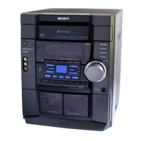
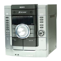
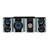
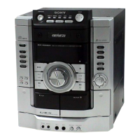
Overview of the main unit with button descriptions.
Step-by-step instructions to set the system clock.
Step-by-step instructions to remove the top case.
Step-by-step instructions to remove the CD door.
Step-by-step instructions to remove the front panel.
Step-by-step instructions to remove the CD mechanism.
Step-by-step instructions to remove the tape mechanism.
Procedures for removing various boards.
Procedure for removing the keyboard board.
Step-by-step instructions to remove the back panel.
Procedures for removing various boards.
Step-by-step instructions to remove the main board.
Step-by-step instructions to remove the power board.
Step-by-step instructions to remove the transformer board.
Procedures for removing boards.
Procedure for removing the spindle motor board.
Step-by-step instructions to remove the optical pick-up.
Procedures for removing boards.
Procedures for removing parts.
Procedure to clear preset data and reset to initial conditions.
Procedures for operating aging mode for CD and tape sections.
Test for fluorescent segments, LEDs, and keyboard functions.
Lists possible error codes for CD and mechanism errors.
Steps to adjust AM IF signal generator to 1000 kHz.
Steps to supply 98 MHz signal and adjust RV101.
Steps to measure voltage and adjust T101.
Identifies adjustment points on the main board.
Procedure to check RF signal level using an oscilloscope.
Identifies component locations on the BD board.
General notes applicable to schematic diagrams.
General notes applicable to PWB diagrams.
Diagrams showing physical layout of circuit boards.
Illustrates signal waveforms at specific IC pins.
Block diagram for the tuner section.
Printed wiring board layout for the CD section.
Second part of the CD section printed wiring board layout.
Schematic diagram for the CD section.
Printed wiring board layout for the main section.
First part of the main section schematic.
Second part of the main section schematic.
Fourth part of the main section schematic.
Printed wiring board layout for the panel section.
Schematic diagram for the panel section.
Printed wiring board layout for power/trans sections.
Schematic diagram for power/trans sections.
Printed wiring board layout for surround/keyboard.
Schematic diagram for surround/keyboard.
Block diagrams for key ICs like LA9242M and LC72131D.
IC block diagram for BA6898FP on the BD board.
IC block diagram for LA1845 on the main board.
IC block diagram for M61519FPD61G on the main board.
IC block diagram for LC72131D on the main board.
IC block diagram for BA6956AN on the driver board.
Detailed pinout and function for IC801 on the panel board.
Exploded view of the main unit assembly.
Exploded view of the front panel assembly.
Exploded view of the main board assembly.
Exploded view of the CD mechanism deck.
Parts list for the address sensor board.
Parts list for the panel section.
Parts list for power and remote sections.
Parts list for the sensor board.
Parts list for the spindle motor.
Parts list for the sub-transformer.
Parts list for the surround section.
Parts list for the transformer section.
Parts list for the main section.
Parts list for the microphone section.
Parts list for the motor components.
Parts list for the panel section.
Parts list for power and remote sections.
Parts list for the sensor section.
Parts list for the spindle motor section.
Parts list for the sub-transformer section.
Parts list for the surround section.
Parts list for the transformer section.
Parts list for the video out section.
| Brand | Sony |
|---|---|
| Model | HCD-RG66 |
| Category | Stereo System |
| Language | English |