10
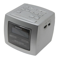
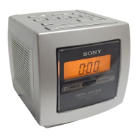
ICF-C112
SECTION 5
DIAGRAMS
THIS NOTE IS COMMON FOR PRINTED WIRING
BOARDS AND SCHEMATIC DIAGRAMS.
Common Note on Schematic Diagram:
• All capacitors are in µF unless otherwise noted. pF: µµF
50 WV or less are not indicated except for electrolytics
and tantalums.
• All resistors are in Ω and
1
/
4
W or less unless otherwise
specified.
•
f
: internal component.
• C : panel designation.
• A : B+ Line.
• H : adjustment for repair.
•Total current is measured with no-signal.
• Power voltage is dc 9V and fed with regulated dc power
supply from battery terminal.
•Voltage is dc with respect to ground under no-signal
(detuned) condition.
no mark : FM
(): AM
•Voltages are taken with a VOM (Input impedance 10 MΩ).
Voltage variations may be noted due to normal produc-
tion tolerances.
• Signal path.
F : FM
f : AM
Note: The components identified by mark 0 or dotted line
with mark 0 are critical for safety.
Replace only with part number specified.
Common Note on Printed Wiring Boards:
• X : parts extracted from the component side.
• Y : parts extracted from the conductor side.
•
f
: internal component.
• : Pattern from the side which enables seeing.
 Loading...