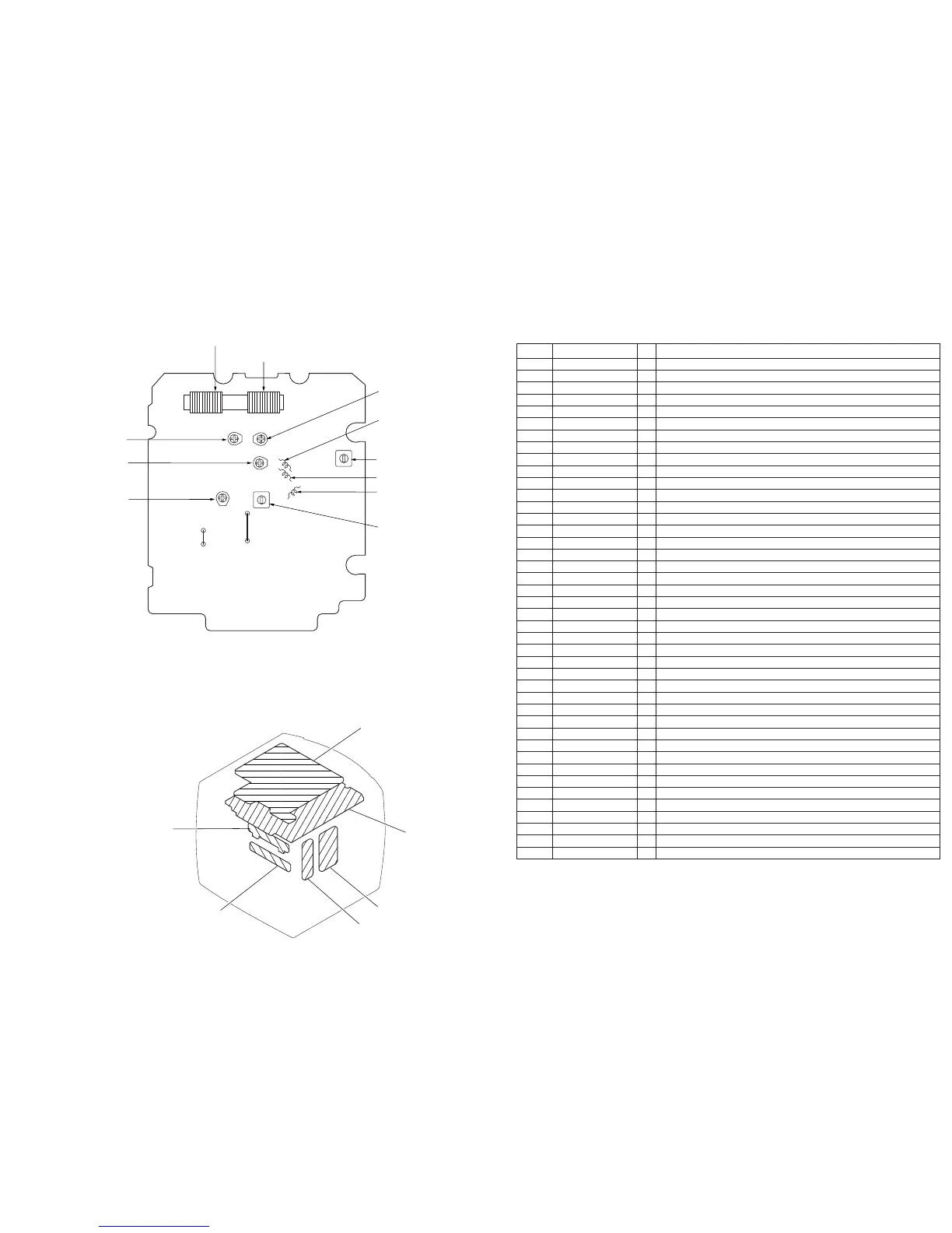
T2 : AM IF Alignment
L3
±
1 : MW Tracking Adjustment
CT4 : LW Tracking
Adjustment
[MAIN BOARD]
(Component side)
L6 : MW Frequency
Coverage Adjustment
L5 : FM Frequency
Coverage Adjustment
CT3 : MW Tracking Adjustment
CT5 : FM Tracking
Adjustment
JW5
GND
VT
JW9
SECTION 4
DIAGRAMS
r
CIRCUIT BOARDS LOCATION
KEY board
MAIN board
SECONDARY board
PRIMARY board
ALARM board
BACK-LIGHT board
Pin No. Pin name I/O Description
1 INIT OUT O Initial output terminal.
2 COLOR1 O LCD back-light drive. “H” : Lighting
3 MUTE O Mute signal output. “L” : Mute ON
4 ALMA O ALARM A LED drive. “H” : Lighting
5 ALMB O ALARM B LED drive. “H” : Lighting
6 KS0 O Key source output terminal.
7 KS1 O Key source output terminal.
8 KS2 O Key source output terminal.
9 KS3 O Key source output terminal.
10 KR0 I Key return input terminal.
11 KR1 I Key return input terminal.
12 KR2 I Key return input terminal.
13 KR3 I Key return input terminal.
14 BAND1 O Band select signal output.
15 BAND2 O Band select signal output.
16 V AMP – Not used (Open).
17 COLOR2 O LCD back-light drive. “H” : Lighting
18 GND – Ground.
19 EO O PLL error output terminal.
20 VCOL I FM/AM local oscillation input terminal.
21 VCOH I TV local oscillation input terminal.
22 VREG1 – Voltage REG terminal for LCD.
23 VDD – Power supply (+2.9V).
24 X OUT O System clock oscillation terminal (75kHz).
25 X IN I System clock oscillation terminal (75kHz).
26 VREG2 – Voltage REG terminal for LCD.
27 VLCD0 – LCD bias terminal.
28 CAPO – LCD bias terminal.
29 CAPI – LCD bias terminal.
30 VLCD1 – LCD bias terminal.
31 COM0 O Common output 0.
32 COM1 O Common output 1.
33 COM2 O Common output 2.
34 COM3 O Common output 3.
35 – 49 LCD0 – 14 O LCD segment drive output.
50 CE I Chip eneble input for LCD load.
51 INT I Intial terminal.
52 BEEP O Beep signal output terminal.
53 – Not used (Open).
54 PB1 I Mode identification terminal.
55 PB2 I Mode identification terminal.
56 PB3 I Mode identification terminal.
4-1. EXPLANATION OF IC TERMINALS
IC3 µPD17071 (LCD DRIVE, SYSTEM CONTROL)