ICF-SW55
4
4
For printed wiring board.
Note:
• z : Through hole.
• :: Pattern from the side which enables seeing.
(The other layers’ patterns are not indicated.)
Caution:
Pattern face side: Parts on the pattern face side seen from the
(Side B) pattern face are indicated.
Parts face side: Parts on the parts face side seen from the
(Side A) parts face are indicated.
• Abbreviation
CND : Canadian model
IT : Italian model
G: Germany model
EA : Saudi Arabia model
• 1AE2, 2AE2 : This shows the differences of the FM/SW frequency bands.
D901 A-3
D902 F-2
D903 B-3
D904 B-2
D905 A-3
D906 A-3
D907 A-4
D908 H-2
D909 H-2
D910 G-3
D911 G-3
D912 G-5
D918 A-2
H901 B-5
H902 B-6
IC901 B-3
IC902 G-4
IC903 C-2
IC904 F-2
IC905 G-2
IC906 C-3
IC907 G-5
IC908 G-5
IC910 H-5
IC911 B-6
IC912 G-3
IC913 G-3
IC914 F-2
IC915 E-2
Q901 A-3
Q902 A-2
Q903 B-5
Q904 H-5
Q905 H-5
Q906 H-2
Q907 H-2
Q908 H-2
Q909 H-2
Q910 H-3
Q911 F-3
Q912 F-3
Q913 G-2
Q914 G-3
Q915 H-2
Q916 A-2
• Semiconductor
Location
Ref. No. Location
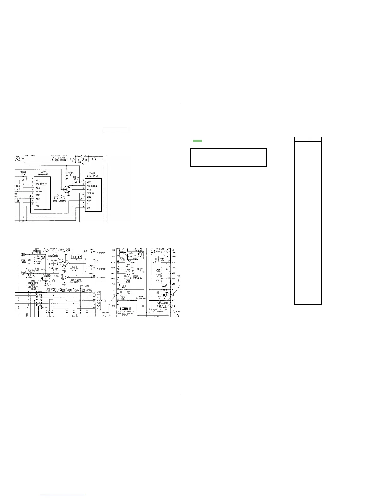
SCHEMATIC DIAGRAM – MICRO COMPUTER SECTION –
page 23 (Location H-I, 17-20)
! : Changed portion
!
!
(Location D-F, 6-13)
!
!
!
!
!
!
!
Last digit : -15