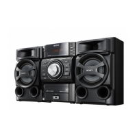
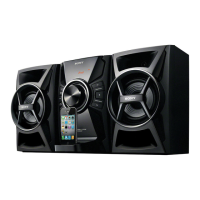
HCD-EC719iP/EC919iP
HCD-EC719iP/EC919iP
1717
For Schematic Diagrams.
Note:
• All capacitors are in μF unless otherwise noted. (p: pF) 50
WV or less are not indicated except for electrolytics and
tantalums.
• All resistors are in Ω and 1/4 W or less unless otherwise
specifi ed.
THIS NOTE IS COMMON FOR PRINTED WIRING BOARDS AND SCHEMATIC DIAGRAMS.
(In addition to this, the necessary note is printed in each block.)
For Printed Wiring Boards.
Note:
• : Pattern from the side which enables seeing.
(The other layers’ patterns are not indicated.)
Caution:
Pattern face side:
(Conductor Side)
Parts face side:
(Component Side)
Parts on the pattern face side seen
from the pattern face are indicated.
Parts on the parts face side seen from
the parts face are indicated.
• Circuit Boards Location
USB board
DOCKING board
POWER board
FRONT board
TUNER board
MAIN boar
Note: The components identifi ed by mark 0 or dotted
line with mark 0 are critical for safety.
Replace only with part number specifi ed.
Note: Les composants identifi és par une marque 0 sont
critiques pour la sécurité.
Ne les remplacer que par une piéce portant le nu-
méro spécifi é.
 Loading...