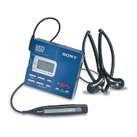
MZ-R500/R500PC
35 35
Pin No. Pin Name I/O Description
223 SPDL MON I Spindle servo monitor signal input
224 – 226 (XAVLS), (SOUND 1, 2) I Not used (open)
227 XHOLD SW I HOLD switch (SW801) input terminal “L”: hold ON, “H”: hold OFF
228 (SYCN REC) I SYNCHRO REC switch input terminal “L”: OFF, “H”: ON Not used (open)
229 (SYNC LEVEL) O Not used (open)
230 PROTECT I
Detection input terminal of the record check claw from the protect detection switch
(S803) “L”: recording possible condition, “H”: protect
231 FLASHVDD — Power supply terminal (for the internal FLASH ROM) (+2.4 V)
232 FLASHVSS — Ground terminal (for the internal FLASH ROM)
233 SLD 1 MON I Sled servo monitor signal input
234 VLON O
Power supply control signal output for the laser diode drive to the power
control (IC901)
235 SLEEP O System sleep control signal coutput to the power control (IC901) “H”: sleep ON
236 FFCLR O Input latch output for the start switching to the power control (IC901)
237 (CHG GAIN) O Charge gain control signal output Not used (open)
238 (CHG) O Charge ON/OFF control signal output “H”: charge ON Not used (open)
239 (TUN REG ON) O Not used (open)
240 XHP STBY O Headphone standby signal output to the headphone amp (IC302)
241 MIFVDD3 — Power supply terminal (for the microcomputer I/F block) (+2.3 V)
242 MIFVSS2 — Ground terminal (for the microcomputer I/F block)
243 (TEST2) O Input terminal for the main test (normally open)
244 NC — Not used (open)
 Loading...