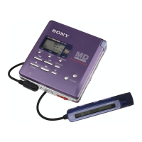
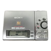
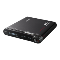
MZ-R5ST
6-4. PRINTED WIRING BOARD — MD MECHANISM SECTION — 6-5. SCHEMATIC DIAGRAM — MD MECHANISM SECTION —
— 41 — — 42 — — 43 — — 44 —
1
2
3
4
5
6
CN401
6P/L1.5
1
2
3
4
5
6
CN402
6P/L1.5
D401
F1J6
D402
F1J6
Q403
2SK2315TY
S
Q401
2SK2315TY
S
S
S
Q402
2SK2315TY
Q404
2SK2315TY
C402
33
4V
TP413
OUTB
TP414
OUTA
TP406
HB
TP403
H-BRIGE
TP405
HA
TP401
GND
C403
220p
100V
C401
0.1
B
OUTA
OUTB
GND
GND
H-BRIGE
H-BRIGE
HA
HB
HR901
(OVER WRITE)
Q401-404
OVER WITE
HEAD DRIVE
1
2
3
4
5
6
CN702
6P/U
Q703
XP6501-TXE
SWITCH
9
10
11
12
13
14
15
16
17
18
1
2
3
4
5
6
7
8
CN701
18P/U
13
14
15
16
17
18
19
20
21
22
23
24
1
2
3
4
5
12
11
10
9
8
7
6
IC701
CXA8048N-ELL200
1
2
3
4
CN001
4P/CLV
S705 (INLIMIT)
S704 (INITIAL)
S703 (REFLECT)
S702 (PROTECT)
S701 (MEDIA)
R705
1 1/10W
R704
1 1/10W
R706 10k
R702
10k
0.50%
R711
0
R703 330
R701
10k
0.50%
TP721
TP722
TP723
TP724
TP725
TP726
TP727
TP728
TP729
TP730
TP731
TP732
TP733
TP734
TP735
TP736
TP737
TP744
TP743
TP742
TP741
TP720
TP719
TP718
TP717
C702
0.047
B
C710
1B
C704
0.1
B
C703
0.022 B
C701 0.022 B
C705 3300p 5%
C706 3300p 5%
C707 3300p 5%
C709
0.1 B
C711
0.1
B
COM
ICOM
U
VS
UIN
VIN
WIN
W
V
BRK+
BRK-
GND
STAT
NC
ICOM
VS
VCC
IBS
IBSET
IB
SLP2
SLp!
STBY
FG
W
V
U
CLV MOTOR
M
M902
(SLED MOTOR)
M
SD-
SD+
1B(B)
2B(B)
2A(A)
1A(A)
COM
U
Y
W
UGND
UGND
INLS
INTSW
REFLCT
PROTECT
PACKIN
SD-
SD+
STCONT
1A(A)
2A(A)
2B(B)
1B(B)
FGIN
2.8V
DIR
VS
MOTOR FOR MODE CONTROL
1
3
5
6
4
2
SPINDLE
MOTOR
DRIVE
M903
(STEPPING MOTOR)
M901
(SPINDLE MOTOR)
MAIN BOARD (1/3)
CN502
(Page 49)
IC701
REC BOARD
CLV BOARD
A
16
0.4
(0)
1.3
(0)
0.4
(0)
0
(0)
2.5
2.5
2.8
2.8
2.7 2.5 2.5 2.8 0.4
0 0.20.20.20.20.20.11.32.70.1 1.1
0.1 0
00
1.4
2.5
2.5
2.2
(0)
2.1
(0)
1.7
(0)
2.2
(0)
2.1
(0)
1.3
(0)
12
A
B
C
D
E
F
345678
• Refer to page 34 for Circuit Boards Location. • Refer to page 77 for IC Block Diagrams.
Ref. No. Location
D401 B-7
D402 B-6
IC701 E-3
Q401 B-7
Q402 A-7
Q403 B-6
Q404 A-6
Q703 D-3
• Semiconductor
Location
Note:
• X : parts extracted from the component side.
•
r
: Through hole.
• b : Pattern from the side which enables seeing.
(The other layers' patterns are not indicated.)
Caution:
Pattern face side: Parts on the pattern face side seen from
(Conductor Side) the pattern face are indicated.
Parts face side: Parts on the parts face side seen from
(Component Side) the parts face are indicated.
Note:
• All capacitors are in µF unless otherwise noted. pF: µµF
50 WV or less are not indicated except for electrolytics and
tantalums.
• All resistors are in Ω and
1
/
4
W or less unless otherwise
specified.
• A : B+ Line.
• Power voltage is dc 4.5 V and fed with regulated dc power
supply from battery terminal.
• Voltages are dc with respect to ground under no-signal
(detuned) conditions.
• Voltages are taken with a VOM (Input impedance 10 MΩ).
Voltage variations may be noted due to normal production
tolerances.
• Signal path.
a : REC
 Loading...