3
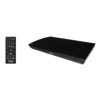
BDP-S7200
Section. Title. Page.
TABLE OF CONTENTS
1. SERVICE NOTE
1-1. Test Disc .....................................................................................1-1
1-2. Drive Repairing .........................................................................1-15
1-2-1. Preparation..............................................................................1-15
1-2-2. Checking Flow ~ Drive (BU) section ~ ....................................1-15
1-2-3. BU Check Flow [zz] ~ ..............................................................1-16
1-2-4. BU (Optical Block) Repair Guide.............................................1-16
1-2-5. BU Adjustment Flow [yy] ~ ......................................................1-17
1-2-6. KEM-480AAA/C2RP2 Packing Spec ......................................1-17
1-2-8. BU Data Decode Jig................................................................1-18
1-2-9. Loading For Service ................................................................1-19
1-2-10.Laser Caution Label ...............................................................1-19
2. DISASSEMBLY
2-1. Disassembly Flow .......................................................................2-1
2-2. Side Panel And Tray Cover Assy ................................................2-1
2-3. Top Panel, FR-1306 Board , FL-1306 Board And Wlan Module .2-2
2-4. Switching Regulator ....................................................................2-2
2-5. MB-1302 Board ...........................................................................2-3
2-6. BD Drive and Foot ...................................................................... 2-3
2-7. Circuit Board Location............................................................... 2-4E
3. BLOCK DIAGRAMS
3-1. Frame Harness ...........................................................................3-1
3-2. Overall Block Diagram ............................................................... 3-2
3-3. Power Block Diagram ............................................................... 3-3E
4. PRINTED WIRING BOARDS
4-1. This Note Is Common For Printed Wiring Boards .......................4-1
4-2. FL-1306 Board (FRONT LEFT) Printed Wiring Board ................4-2
4-3. FR-1306 Board (FRONT RIGHT) Printed Wiring Board .............4-2
4-4. MB-1302 Board(MAIN) Printed Wiring Board (Side A) ............... 4-3
4-5. MB-1302 Board (MAIN) Printed Wiring Board (Side B) ............4-4E
5. SERVICE MODE AND ERROR LOG LIST .................... 5-1
6. TROUBLESHOOTING ................................................... 6-1
7. REPAIR PARTS LIST
7-1. Exploded Views ..........................................................................7-1
7-1-1. Case Section ............................................................................. 7-1
7-1-2. Main Chassis Section................................................................7-2
7-1-3. BD Section ................................................................................7-3
7-1-4. Accessories ...............................................................................7-4
 Loading...