3
SA-VE322/VE325/WMS325/SS-CN325/V325
SECTION 1
DIAGRAMS
1-1. NOTE FOR PRINTED WIRING BOARDS AND SCHEMATIC DIAGRAMS
Note on Printed Wiring Board:
• : Pattern from the side which enables seeing.
• Abbreviation
AR : Argentina model
SP : Singapore model
Note on Schematic Diagram:
• All capacitors are in µF unless otherwise noted. pF: µµF
50 WV or less are not indicated except for electrolytics
and tantalums.
• All resistors are in Ω and
1
/
4
W or less unless otherwise
specified.
• 2 : nonflammable resistor.
• C : panel designation.
• A : B+ Line.
• B : B– Line.
• Voltages are dc with respect to ground under no-signal
conditions.
• Voltages are dc with respect to ground in service mode.
no mark : MUSIC MODE
( ) : MOVIE MODE
• Voltages are taken with a VOM (Input impedance 10 MΩ).
Voltage variations may be noted due to normal produc-
tion tolerances.
• Signal path.
F : AUDIO
• Abbreviation
AR : Argentina model
AUS : Australian model
CH : Chinese model
CND : Canadian model
MX : Mexican model
SP : Singapore model
Note:
The components identi-
fied by mark 0 or dotted
line with mark 0 are criti-
cal for safety.
Replace only with part
number specified.
Note:
Les composants identifiés par
une marque 0 sont critiques
pour la sécurité.
Ne les remplacer que par une
pièce portant le numéro
spécifié.
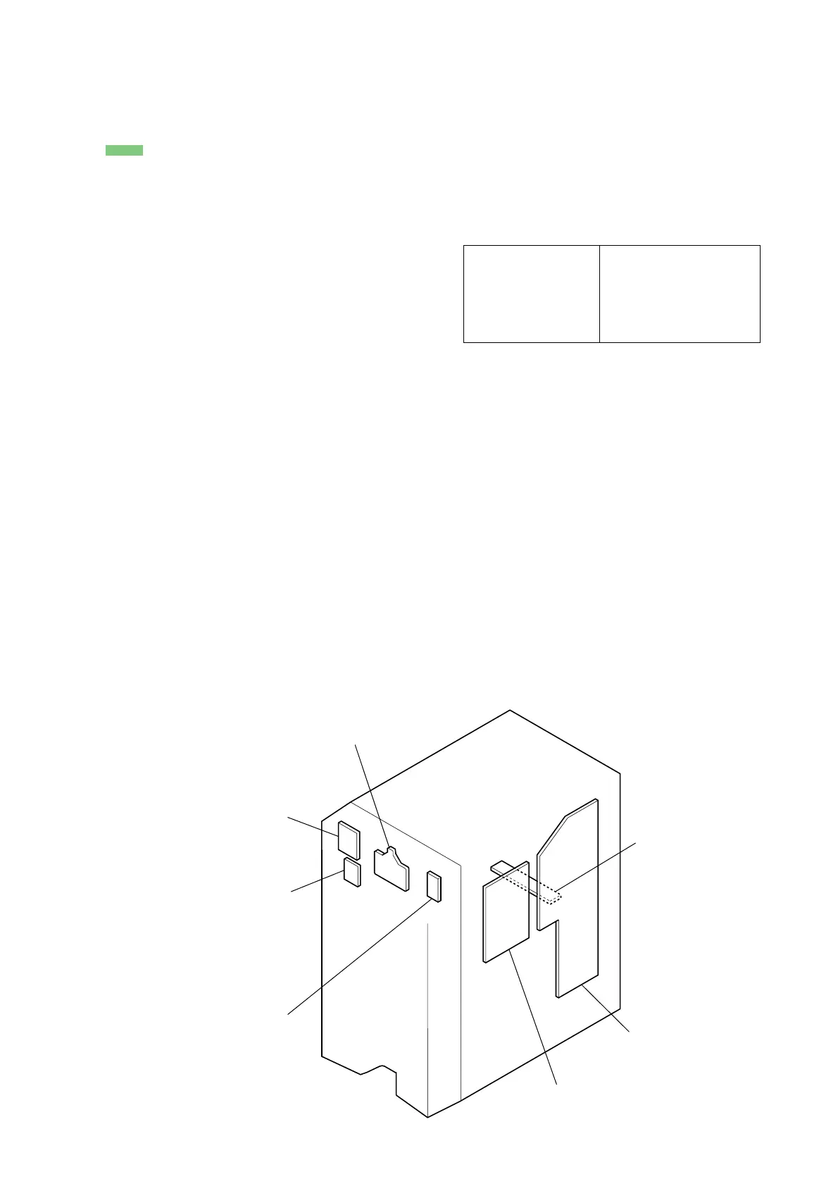
• Circuit Boards Location
(SA-WMS325)
MAIN board
POWER board
AUTO POWER board
POWER SWITCH board
CONTROL board
CONNECTOR board
MODE board