SA-WCT800
26
• IC Pin Function Description
SUB-MAIN BOARD IC7400 MB9AF142LBPMC1-G-JNE2 (SYSTEM CONTROLLER)
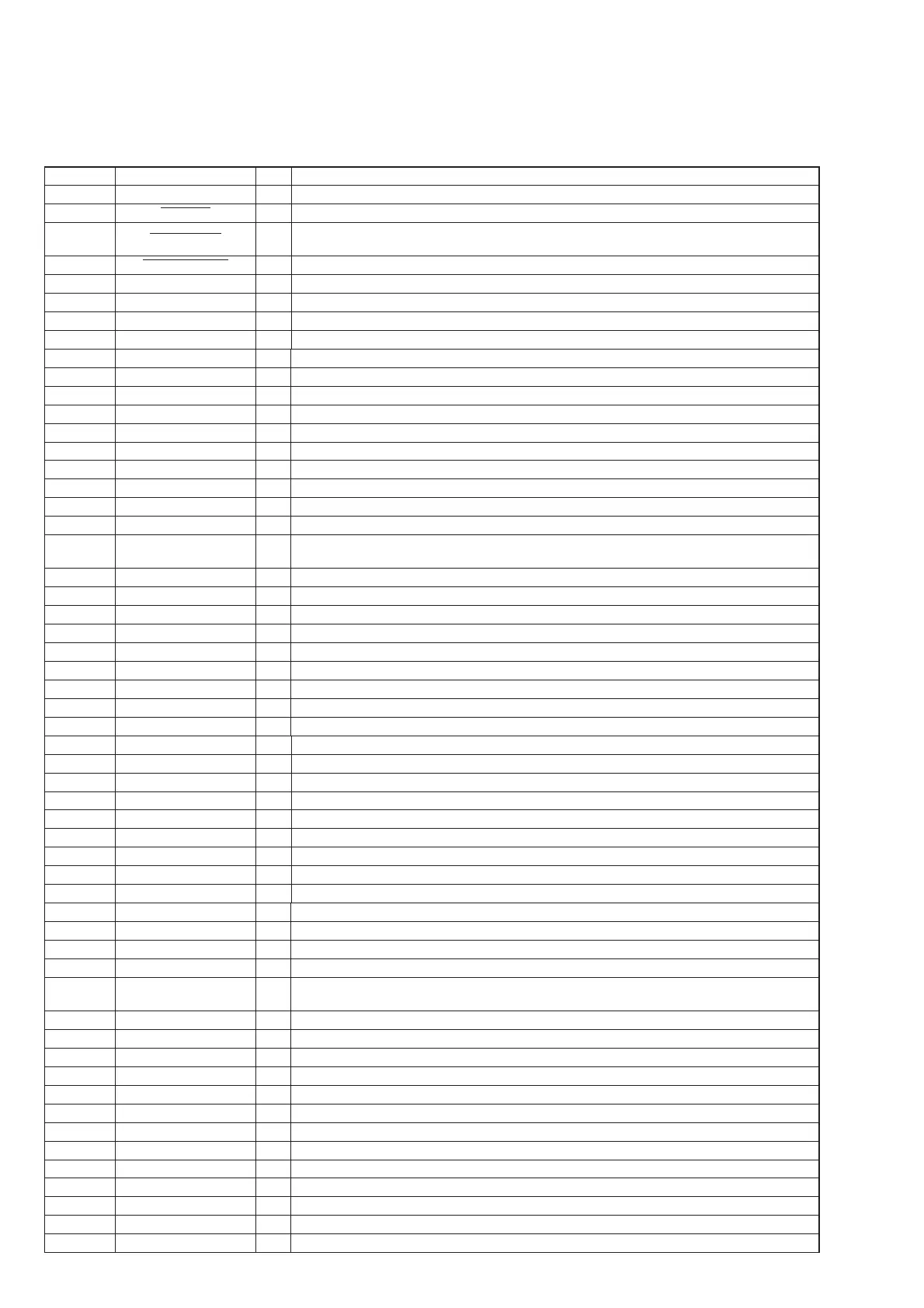
Pin No. Pin Name I/O Description
1 VCC - Power supply terminal (+3.3V)
2 DC_DET
I Speaker DC detection signal input terminal “L”: speaker DC is detected
3 DRIVER_SD
I
Shutdown signal input from the digital power amplifi er, power detect circuit and thermal detect
circuit “L”: shutdown
4 P_DAMP_CLIP
I Clipping warning signal input from the digital power amplifi er “L”: clipping
5 - - Not used
6 TAS5534_SCL O Serial data transfer clock signal output to the stream processor
7 TAS5534_SDA I/O Two-way data bus with the stream processor
8 - - Not used
9 TAS5534_XPDN O Power down signal output to the stream processor “L”: power down
10 TAS5534_XRST O Rest signal output to the stream processor “L”: reset
11 TAS5534_MUTE O Muting on/off control signal output to the stream processor “L”: muting on
12, 13 - - Not used
14 LED_RED O LED drive signal output terminal for the on/standby indicator (red) “H”: LED on
15 LED_GREEN O LED drive signal output terminal for the on/standby indicator (green) “H”: LED on
16 VSS - Ground terminal
17 C - External capacitor connection terminal
18 VCC - Power supply terminal (+3.3V)
19, 20 - - Not used
21 INITX (RESET) I
System reset signal input terminal “L”: reset
For several hundreds msec. after the power supply rises, “L” is input, then it change to “H”
22, 23 - - Not used
24 WS_RST O Reset signal output to the RF modulator “L”: reset
25 WS_SCL O Serial data transfer clock signal output to the RF modulator
26 WS_SDA I/O Two-way data bus with the RF modulator
27 WS_INT I Interrupt signal input from the RF modulator
28 MD1 I Mode selection signal input terminal “L”: fl ash memory writing mode
29 MD0 I Mode selection signal input terminal “H”: fl ash memory writing mode
30 X0 I System clock input terminal (4 MHz)
31 X1 O System clock output terminal (4 MHz)
32 VSS - Ground terminal
33 VCC - Power supply terminal (+3.3V)
34 KEY_PAIRING I LINK key input terminal
35 KEY_POWER I Power key input terminal
36 MODEL I Model setting terminal
37 DEST I Destination setting terminal
38 Pull Up Power O Power supply control terminal for the destination setting
39 - - Not used
40 AC_CUT I AC cut detection signal input terminal “L”: AC cut is detected
41 AVCC - Power supply terminal (+3.3V)
42 AVRH I Reference voltage (+3.3V) input terminal
43 AVSS - Ground terminal
44, 45 P_CONT1, P_CONT2 O Power on/off control signal output terminal “H”: power on
46
ON CHIP DEBUG/
CLK1
I Serial data transfer clock signal input terminal for fl ash memory writing
47 (PROG VUTX) O Serial data output terminal for fl ash memory writing
48 (PROG VURX) I Serial data input terminal for fl ash memory writing
49 - - Not used
50 TCK I Test clock signal input terminal (for JTAG) Not used
51 TDI I Test data input terminal (for JTAG) Not used
52 TMS I Test mode selection signal input terminal (for JTAG) Not used
53 TDO O Test data output terminal (for JTAG) Not used
54 to 59 - - Not used
60 PVDD_STBY O Power standby signal output terminal Not used
61 VCC - Power supply terminal (+3.3V)
62 PVDD_SD_EN O Not used
63 - - Not used
64 VSS - Ground terminal


 To Next Page