– 6 –
SECTION 4
DIAGRAMS
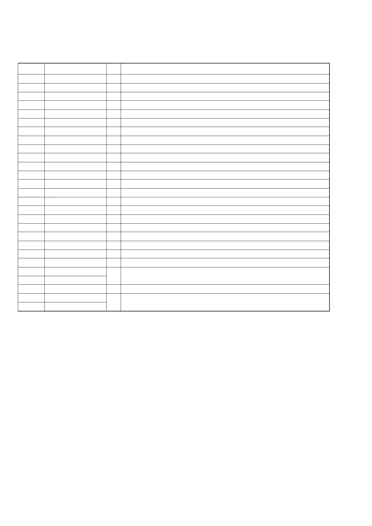
4-1. EXPLANATION OF IC TERMINALS
IC301 µ PD17015GS-556-GJG (SYSTEM CONTROL, LCD DRIVE)
Pin No. Pin name I/O Description
1 POB2 I Key return input.
2 PCO0 O Key source output.
3 PCO1 O Key source output.
4 PCO2 I Power (AUTO OFF) key input.
5 PCO3 I HOLD key input.
6 POD0/BEEP O Beep output.
7 POA0 I Key return input (Fixed at “L”).
8 POA1 I Voltage decrease information input. E : On-and-off
9 POA2 O Power ON/OFF output. “H” : ON
10 POA3 O Mute signal output. “H” : Mute ON
11 CE I Voltage decrease information input. E : Lighting
12 XOUT O System clock output (75 kHz).
13 XIN I System clock input (75 kHz).
14 VDD — Power supply.
15 GND — Ground.
16 EO O PLL error output.
17 VREG O Voltage regulator output.
18 VCOH I FM VCO input.
19 VCOL — Not used (OPEN).
20 – 28 LCD 0 – 8 O LCD segment output.
29 – 32 COM 0 – 3 O LCD common output.
33 VLCD1 — Power supply for LCD drive.
34 CAP1
— Connecting pins of the capacitor for LCD drive voltage.
35 CAP0
36 VLCD0 — Power supply for LCD drive.
37 POB0
I Key return input.
38 POB1