25
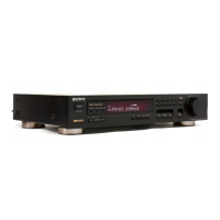
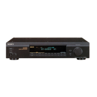
ST-S3
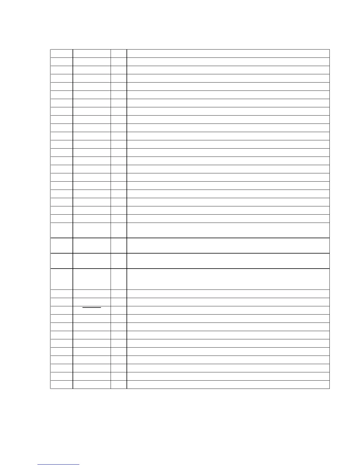
• PANEL BOARD IC601 MB90M407PF-G-102-BND (DISPLAY CONTROLLER)
Pin No. Pin Name I/O Description
1 to 6 G6 to G1 O
Grid drive signal output to the fluorescent indicator tube (FL601)
7 to 10 A1 to A4 O
Segment drive signal output to the fluorescent indicator tube (FL601)
11 VSS FOR IO —
Ground terminal (for I/O)
12 to 22 A5 to A15 O
Segment drive signal output to the fluorescent indicator tube (FL601)
23 VDD FOR VFT —
Power supply terminal (+3.3V) (for VFT)
24 to 41 A16 to A33 O
Segment drive signal output to the fluorescent indicator tube (FL601)
42 VSS FOR IO —
Ground terminal (for I/O)
43 to 47 A34 toA38 O
Segment drive signal output to the fluorescent indicator tube (FL601)
48 VKK FOR VFT —
Power supply terminal (–28V) (for VFT)
49 MODE0 —
Chip mode selection terminal Not used (fixed at “H”)
50 MODE1 —
Chip mode selection terminal Not used (fixed at “H”)
51 MODE2 —
Chip mode selection terminal Not used (fixed at “L”)
52 JOG2B I
Jog dial pulse input from the rotary encoder (for sound) in the TA-S3 (B phase input)
53 JOG2A I
Jog dial pulse input from the rotary encoder (for sound) in the TA-S3 (A phase input)
54 JOG1B I
Jog dial pulse input from the rotary encoder (for function) in the TA-S3 (B phase input)
55 JOG1A I
Jog dial pulse input from the rotary encoder (for function) in the TA-S3 (A phase input)
56 VOLA I
Jog dial pulse input from the rotary encoder (for volume) in the TA-S3 (A phase input)
57 VOLB I
Jog dial pulse input from the rotary encoder (for volume) in the TA-S3 (B phase input)
58, 59 ——
Not used (open)
60 I2C DATA I/O
Communication data bus with the system controller (IC501) and CDP-S3
61 I2C CLK I/O
Communication data reading clock signal input or transfer clock signal output with the system
controller (IC501) and CDP-S3
62
AVCC FOR
ANALOG
—
Power supply terminal (+3.3V) (for analog)
63
AVSS FOR
ANALOG
—
Ground terminal (for analog)
64 KEY0 I
Key input terminal (A/D input) CLOCK/TIMER, TIMER SELECT, TUNER/BAND, TUNING
+/–, ENTER, PRESET +/–, TUNER MEMORY, STEREO/MONO, PTY (S602 to S612) keys
input
65 KEY1 I
Key input terminal for TA-S3 (A/D input)
66 to 76 ——
Not used (open)
77 RESET I
Reset signal input from the system controller (IC501) “L”: reset
78 to 80 ——
Not used (open)
81 VSS FOR CPU
— Ground terminal (for CPU)
82 XIN I
System clock input terminal (4 MHz)
83 XOUT O
System clock output terminal (4 MHz)
84 VCC FOR CPU
— Power supply terminal (+3.3V)
85 to 91 ——
Not used (open)
92 to 94 G12 O
Grid drive signal output to the fluorescent indicator tube (FL601)
95 to 98 G11 to G8 O
Grid drive signal output to the fluorescent indicator tube (FL601)
99, 100 G7 O
Grid drive signal output to the fluorescent indicator tube (FL601)
 Loading...