STR-DG710
2424
STR-DG710
for schematic diagram:
• All capacitors are in µF unless otherwise noted. (p: pF)
50 WV or less are not indicated except for electrolytics
and tantalums.
• All resistors are in Ω and
1
/
4
W or less unless otherwise
specified.
•
f
: internal component.
• 2 : nonflammable resistor.
• 5 : fusible resistor.
• C : panel designation.
• A : B+ Line.
• B : B– Line.
•Voltage and waveforms are dc with respect to ground
under no-signal (detuned) conditions.
no mark : FM
•Voltages are taken with a VOM (Input impedance 10 MΩ).
Voltage variations may be noted due to normal produc-
tion tolerances.
•Waveforms are taken with a oscilloscope.
Voltage variations may be noted due to normal produc-
tion tolerances.
• Circled numbers refer to waveforms.
• Signal path.
F : TUNER (FM/AM)
L : VIDEO (AUDIO)
I : VIDEO
J : DVD (DIGITAL)
c : CD (ANALOG)
• Abbreviation
AUS : Australian model.
CND : Canadian model.
MY : Malaysia model.
SP : Singapore model.
TH : Thai model.
for printed wiring boards:
• X : parts extracted from the component side.
•
f
: internal component.
• : Pattern from the side which enables seeing.
Caution:
Pattern face side: Parts on the pattern face side seen from the
(Side B) pattern face are indicated.
Parts face side: Parts on the parts face side seen from the
(Side A) parts face are indicated.
C
B
These are omitted.
E
Q
B
These are omitted.
C
Q
Q
E
BCE
THIS NOTE IS COMMON FOR PRINTED WIRING BOARDS AND SCHEMATIC DIAGRAMS.
(In addition to this, the necessary note is printed in each block.)
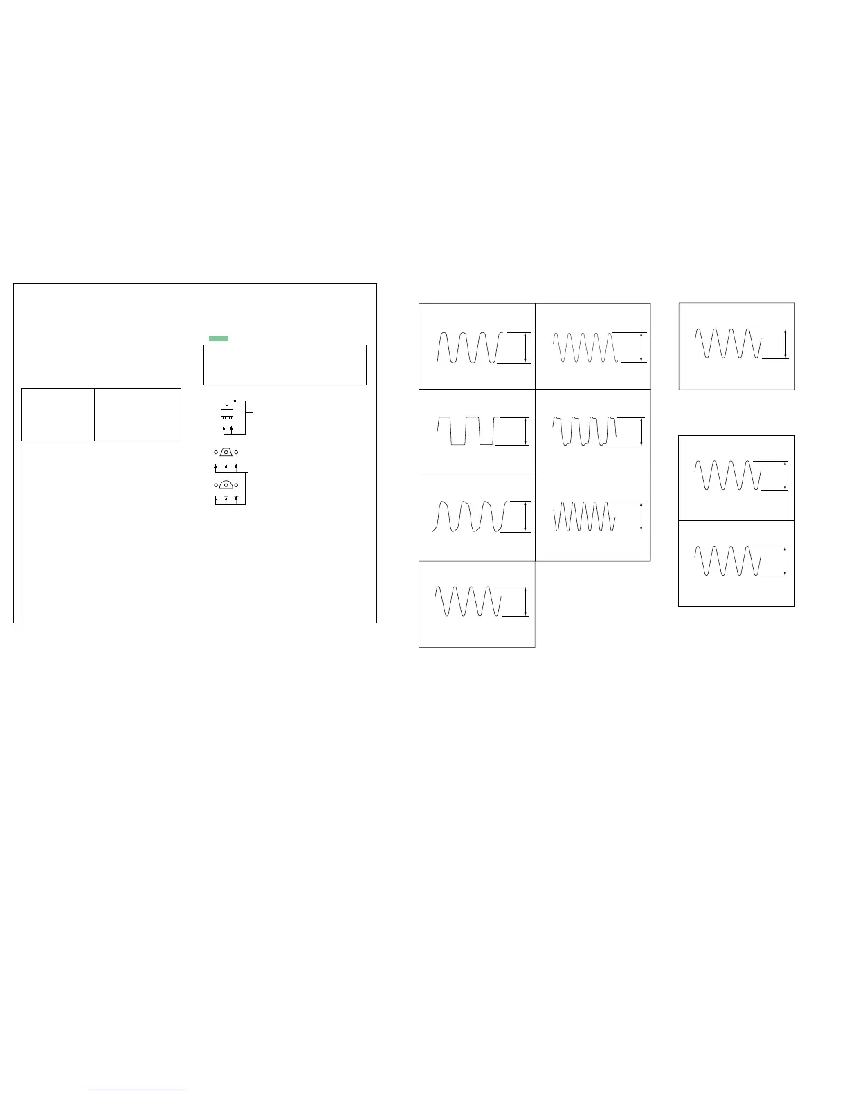
• Waveforms
— DIGITAL Board — — XM Board —
1
IC102 wh (OSCOUT)
0.07 Vp-p
0.05 V/DIV, 0.2
µ
sec/DIV
45.158 MHz
Note:
The components identi-
fied by mark 0 or dotted
line with mark 0 are criti-
cal for safety.
Replace only with part
number specified.
Note:
Les composants identifiés par
une marque 0 sont critiques
pour la sécurité.
Ne les remplacer que par une
piéce portant le numéro
spécifié.
• Abbreviation
AUS : Australian model.
CND : Canadian model.
MY : Malaysia model.
SP : Singapore model.
TH : Thai model.
1
IC1301 qd (CKOUT)
3.8 Vp-p
3.1 Vp-p
1 V/DIV, 50 nsec/DIV
3
IC1301 wa (XOUT)
1 V/DIV, 50 nsec/DIV
4
IC1501 9 (MCLK1)
1.7 Vp-p
1 V/DIV, 50 nsec/DIV
2
IC1301 qf (BCK)
3.6 Vp-p
1 V/DIV, 0.2
µ
s/DIV
13.9 MHz
12.288 MHz
3.07 MHz
12.288 MHz
5
IC1501 qs (MCLK2)
3.2 Vp-p
2.8 Vp-p
1 V/DIV, 50 nsec/DIV
7
IC1907 tj (X1)
1 V/DIV, 50 nsec/DIV
6
IC1501 qf (SCKOUT)
3.5 Vp-p
1 V/DIV, 50 nsec/DIV
12.5 MHz
12.288 MHz
13.9 MHz
— HDMI RE Board —
2.2 Vp-p
1 V/DIV, 20 nsec/DIV
28.322 MHz
1
IC3511 if (XTALOUT)
3.4 Vp-p
1 V/DIV, 50 nsec/DIV
10 MHz
2
IC3519 qa (XOUT)
Ver. 1.1