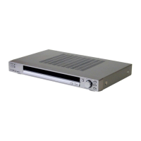
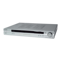
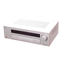
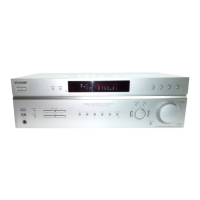
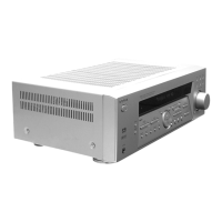
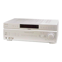
STR-KSL40/SL40
2
S/N
Mono: 76 dB
Stereo: 70 dB
Harmonic distortion at 1 kHz
Mono: 0.3%
Stereo: 0.5%
Separation 45 dB at 1 kHz
Frequency response 30 Hz – 15 kHz
+0.5/–2 dB
Selectivity 60 dB at 400 kHz
AM tuner section
Tuning range
Models of area code CEL, CEK
With 9-kHz tuning scale: 531 – 1602 kHz
Antenna Loop antenna
Intermediate frequency 450 kHz
Usable sensitivity 50 dB/m (at 999 kHz)
S/N 54 dB (at 50 mV/m)
Harmonic distortion 0.5% (50 mV/m, 400 Hz)
Selectivity At 9 kHz: 35 dB
General
Power requirements
Area code Power requirements
CEL, CEK 230 V AC, 50/60 Hz
Power consumption
Area code Power consumption
CEL, CEK 130 W
Power consumption (during standby mode)
0.3 W
Dimensions (w/h/d) 430 x 56 x 288 mm
including projecting parts and controls
Mass (Approx.) 4.5 kg
Supplied accessories (STR-SL40)
FM wire antenna (1)
AM loop antenna (1)
Remote commander RM-U40 (1)
R6 (size-AA) batteries (2)
Speakers plugs (5)
Hexagon wrench (1)
Design and specifications are subject to change without notice.
Unleaded solder
Boards requiring use of unleaded solder are printed with the lead-
free mark (LF) indicating the solder contains no lead.
(Caution: Some printed circuit boards may not come printed with
the lead free mark due to their particular size.)
: LEAD FREE MARK
Unleaded solder has the following characteristics.
• Unleaded solder melts at a temperature about 40°C higher than
ordinary solder.
Ordinary soldering irons can be used but the iron tip has to be
applied to the solder joint for a slightly longer time.
Soldering irons using a temperature regulator should be set to
about 350°C.
Caution: The printed pattern (copper foil) may peel away if the
heated tip is applied for too long, so be careful!
• Strong viscosity
Unleaded solder is more viscous (sticky, less prone to flow) than
ordinary solder so use caution not to let solder bridges occur
such as on IC pins, etc.
• Usable with ordinary solder
It is best to use only unleaded solder but unleaded solder may
also be added to ordinary solder.
Notes on chip component replacement
• Never reuse a disconnected chip component.
• Notice that the minus side of a tantalum capacitor may be dam-
aged by heat.
TABLE OF CONTENTS
SAFETY-RELATED COMPONENT WARNING!!
COMPONENTS IDENTIFIED BY MARK 0 OR DOTTED LINE
WITH MARK 0 ON THE SCHEMATIC DIAGRAMS AND IN THE
PARTS LIST ARE CRITICAL TO SAFE OPERATION. REPLACE
THESE COMPONENTS WITH SONY PARTS WHOSE PART NUM-
BERS APPEAR AS SHOWN IN THIS MANUAL OR IN SUPPLE-
MENTS PUBLISHED BY SONY.
Specifications ............................................................................ 1
1. GENERAL ...................................................................... 3
2. TEST MODE ................................................................. 4
3. DIAGRAMS
3-1. IC Pin Function Descriptions .................................. 6
3-2. Block Diagrams – Main Section – ........................ 10
Block Diagrams – Display/Power Section – ......... 11
3-3. Printed Wiring Boards
– Digital Section (Side A)– ................................... 12
Printed Wiring Boards
– Digital Section (Side B)– ................................... 13
3-4. Schematic Diagram – Digital Section (1/3)– ........ 14
3-5. Schematic Diagram – Digital Section (2/3)– ........ 15
3-6. Schematic Diagram – Digital Section (3/3)– ........ 16
3-7. Printed Wiring Boards – Main Section– ............... 17
3-8. Schematic Diagram – Main Section (1/2)– .......... 18
3-9. Schematic Diagram – Main Section (2/2)– .......... 19
3-10. Printed Wiring Boards – Display Section– ........... 20
3-11. Schematic Diagram – Display Section– ............... 21
3-12. IC Block Diagrams ................................................ 22
4. EXPLODED VIEWS
4-1. Front Panel Section ................................................. 23
4-2. Cabinet Section ........................................................ 24
5. ELECTRICAL PARTS LIST .................................... 25