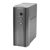
(CN111)
3
claw
2
three screws
(BVTP3
×
8)
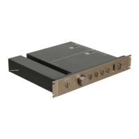
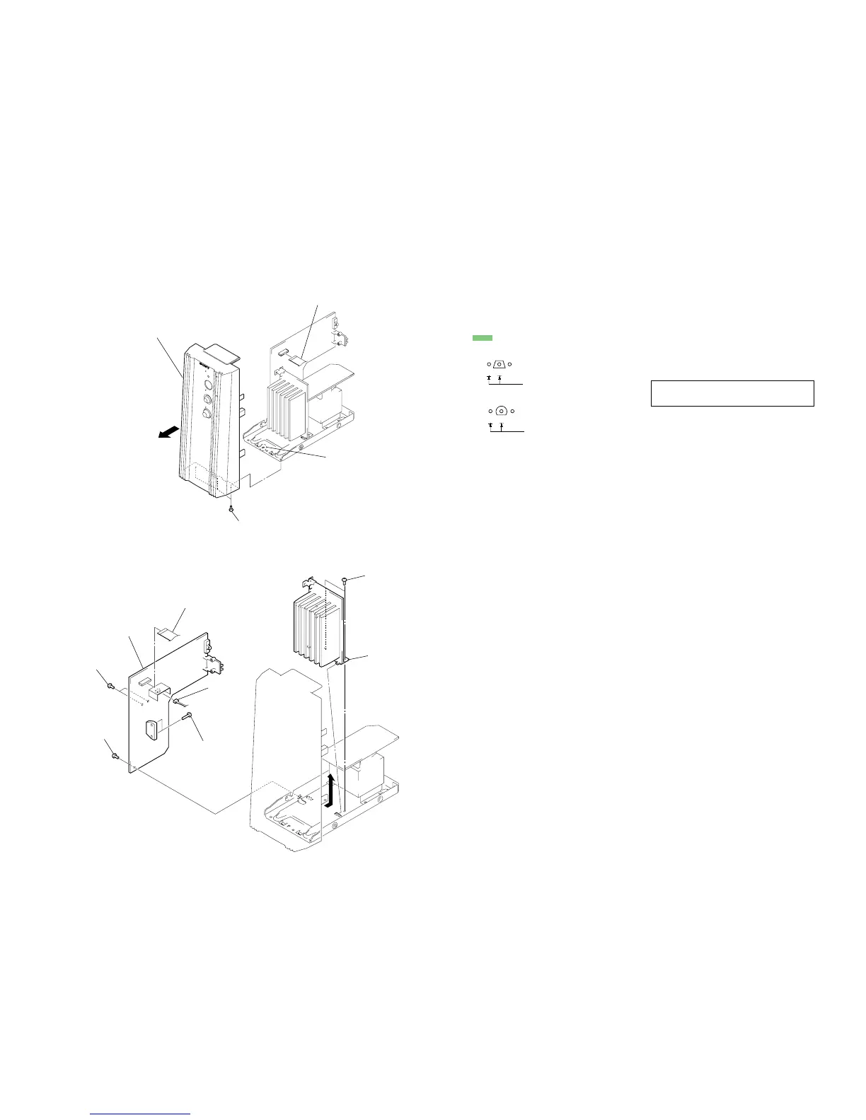
3-4. MAIN BOARD
SECTION 4
DIAGRAMS
4-1. NOTE FOR PRINTED WIRING BOARDS AND SCHEMATIC DIAGRAMS
Note on Printed Wiring Board:
• X : parts extracted from the component side.
• Y : parts extracted from the conductor side.
• : Pattern from the side which enables seeing.
• Indication of transistor.
Note on Schematic Diagram:
• All capacitors are in µF unless otherwise noted. pF: µµF
50 WV or less are not indicated except for electrolytics
and tantalums.
• All resistors are in Ω and
1
/
4
W or less unless otherwise
specified.
• 2 : nonflammable resistor.
• 5 : fusible resistor.
• C : panel designation.
• A : B+ Line.
• B : B– Line.
• Voltages are dc with respect to ground under no-signal
conditions.
• Voltages are taken with a VOM (Input impedance 10 MΩ).
Voltage variations may be noted due to normal produc-
tion tolerances.
no mark : POWER ON
• Signal path.
F : AUDIO
• Abbreviation
BR : Brazilian model
E91 : 220 V AC area in E model
MX : Mexican model
Note: The components identified by mark 0 or dotted line
with mark 0 are critical for safety.
Replace only with part number specified.
• Abbreviation
E91 : 220 V AC area in E model
MX : Mexican model
 Loading...