EasyManua.ls Logo

Sony TA-D505 Service Manual

Sony TA-D505
21 pages
To Next Page IconTo Next Page
Page #1 background imageLoading...
Page #1 background image
SERVICE
MANUAL
SPECIFICATIONS
Continuous
RMS
power
output
60
W
+
60
W
(6
ohms,
at
1
kHz,
5%
THD)
50W
+
50
W
(6
ohms,
DIN,
1
kHz)
90
W
+
90
W
(6
ohms,
at
1
kHz,
10%
THD)
Music
power
output
Input.
Jack
type
|
PHONO
(MM)
VIDEO1
47
kohms
VIDEO2
47
kohms
CD
47
kohms
MIC
10
kohms
Output.
Jack
type
Voltage
SURROUND
|
Phono
SPEAKER
Sensitivity
Impedance
47
kohms
Impedance
Accepts
speakers
of
16
ohms
Accepts
headphones
of
8
ohms
or
more
Frequency
response
Power
requirements
Power
consumption
AC
outlet
Weight
Dimensions
TA-Do0a
AEP
Model
UK
Model
E
Model
Australian
Model
15
Hz
to
50
kHz
+3.
dB
220-230
V
AC,
50/60
Hz
150
W
1
unswitched,
100
W
max.
Approx.
8
kg
(17
lbs
11
02z)
Approx.
355
132.5
x
320
mm
(w/h/d,
including
projections)
(14
X
51/4
X
12
5/g
inches)
Design
and
specifications
subject
to
change
without
notice.
Note
This
appliance
conforms
with
EEC
Directive
87/308/EEC
regarding
interference
suppression.
STEREO
AMPLIFIER
SONY.
Question and Answer IconNeed help?

Do you have a question about the Sony TA-D505 and is the answer not in the manual?

Sony TA-D505 Specifications

General IconGeneral
BrandSony
ModelTA-D505
CategoryAmplifier
LanguageEnglish

Summary

Specifications

Safety Check-Out and Warnings

Leakage Test Procedure

Procedure for testing AC leakage from exposed metal parts to earth ground and between parts.

Safety-Related Component Warning

Identifies critical safety components and replacement guidelines for safe operation.

General Information and Controls

Amplifier Front Panel Controls

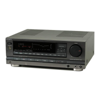
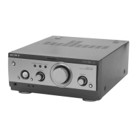
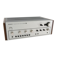
Description and numbering of front panel controls for the amplifier unit, including power and function selectors.

Diagrams and Schematics

IC Pin Function Details

Details pin assignments and functions for system controller IC708.

IC Block Diagrams

Visual representations of internal IC circuit configurations and pinouts.

Circuit Board Locations

Diagrams illustrating the physical placement of various circuit boards within the unit.

Semiconductor Lead Layouts

Illustrations showing the physical pin configurations of common semiconductor components.

Printed Wiring Board Layouts

Detailed diagrams of the printed circuit board layouts for schematic reference.

Exploded Views and Parts Breakdown

Cabinet Section Exploded View

Diagram showing the assembly and parts breakdown of the unit's exterior cabinet.

Main Board Section Exploded View

Diagram illustrating the assembly and parts breakdown of the main internal circuit board.

Electrical Parts List

Related product manuals