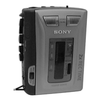
TCS-100DV
– 21 –
– 22 –
– 23 –
– 24 –
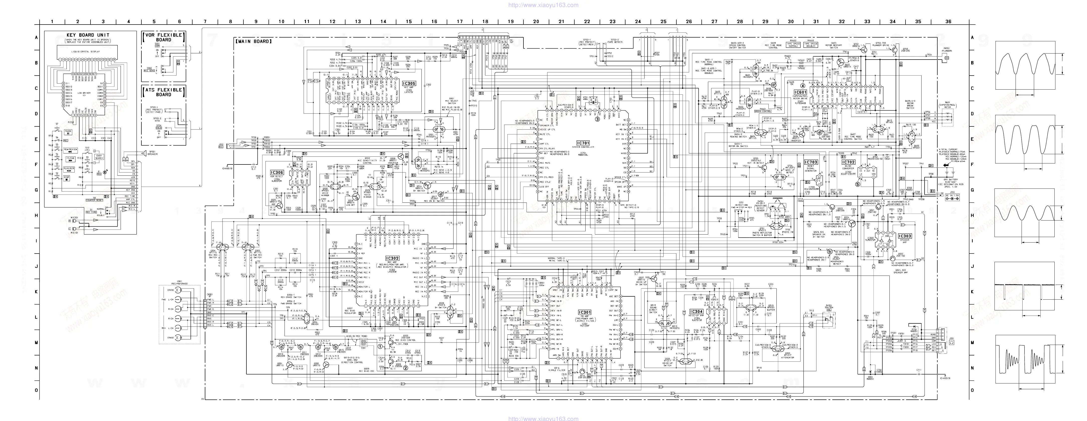
6-4. SCHEMATIC DIAGRAM • See page 25 for IC Block Diagrams.
430 mVp-p
4.6 ms
1.3 Vp-p
17.5
µs
41 mVp-p
17.5 µs
• Waveforms
1 Q333 (emitter) (REC mode)
20 mV/DIV, 10 µs/DIV
2 Q309 (base) (REC mode)
500 mV/DIV, 10 µs/DIV
3 IC701 5 (XO)
2 V/DIV, 100 ns/DIV
4 IC601 wl (PULSE)
200 mV/DIV, 2 ms/DIV
4 Vp-p
10.5 µs
5 IC702 4 (LX)
1 V/DIV, 2 µs/DIV
Note on Schematic Diagram:
• All capacitors are in µF unless otherwise noted. pF: µµF
50 WV or less are not indicated except for electrolytics
and tantalums.
• All resistors are in Ω and
1
/
4
W or less unless otherwise
specified.
•
f
: internal component.
• C : panel designation.
• U : B+ Line.
• H : adjustment for repair.
• AC voltage readings in the REC bias oscillator with a level
meter.
• Power voltage is dc 1.5 V and fed with regulated dc power
supply from battery terminal.
• Voltages and waveforms are dc with respect to ground
under no-signal conditions.
no mark : PB (F: FWD, R: REV)
( ) : REC (F: FWD, R: REV)
〈〈 〉〉 : DOUBLE REC
[ ] : VOICE-UP PB
{ } : REC PAUSE (VOR)
∗
: Impossible to measure
• Voltages are taken with a VOM (Input impedance 10 MΩ).
Voltage variations may be noted due to normal produc-
tion tolerances.
• Waveforms are taken with a oscilloscope.
Voltage variations may be noted due to normal produc-
tion tolerances.
• Circled numbers refer to waveforms.
• Signal path.
E : PB
a : REC
N : MIC
w
w
w
.
x
i
a
o
y
u
1
6
3
.
c
o
m
Q
Q
3
7
6
3
1
5
1
5
0
9
9
2
8
9
4
2
9
8
T
E
L
1
3
9
4
2
2
9
6
5
1
3
9
9
2
8
9
4
2
9
8
0
5
1
5
1
3
6
7
3
Q
Q
TEL 13942296513 QQ 376315150 892498299
TEL 13942296513 QQ 376315150 892498299
http://www.xiaoyu163.com
http://www.xiaoyu163.com
 Loading...