Do you have a question about the Sony Trinitron KV-SW29M50 and is the answer not in the manual?
Overview of the TV's internal functional blocks and signal flow.
Detailed circuit diagram for the C board, covering RGB amplification and rotation.
Circuit diagram for the H5 (Front Panel) board, detailing connections and components.
Schematic for the VM (Velocity Modulation) board, showing its circuit components and layout.
Circuit diagram for the D3 board, responsible for Dynamic Focus and DQP functions.
Schematic for the J3 (DVD Terminal) board, detailing its connections and components.
Circuit diagrams for the F (CISPR) and H4 (Front Panel) boards.
Schematic for the B board (AV SW) covering audio switching functions.
Circuit diagram for the K board (Karaoke), detailing audio processing components.
Schematic for the A board's processor, audio, tuner, and jack sections.
Circuit diagram for the A board's power supply and deflection systems.
Printed wiring layout for the A board, covering multiple functional blocks.
Printed wiring diagram for the C board's video processing and picture correction.
Printed wiring layout for the H5 board, representing the front panel components.
Printed wiring diagram for the J3 board, associated with DVD input/output.
Printed wiring layout for the B board, handling AV switching functions.
Printed wiring diagram for the K board, related to karaoke audio processing.
Printed wiring layout for the H4 board, associated with the front panel interface.
Printed wiring diagram for the VM board, controlling velocity modulation.
Printed wiring layout for the D3 board, managing focus and DQP circuits.
Printed wiring diagram for the F board, related to CISPR filtering.
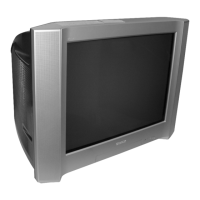
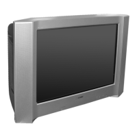
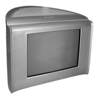
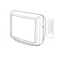
| Screen Size | 29 inches |
|---|---|
| Display Type | CRT |
| Aspect Ratio | 4:3 |
| Sound System | NICAM/A2 |
| Input/Output Terminals | S-Video |