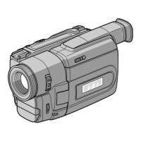
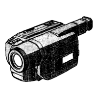
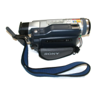
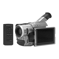
Do you have a question about the Sony TRV510 and is the answer not in the manual?
Details on video recording, audio, signal, cassette, and timing parameters.
Optical zoom, focal length, filter diameter, color temperature, minimum illumination, and CCD details.
Lists various input and output ports like S-Video, DV, Audio, and Headphone jacks.
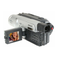
Details the size, resolution, and dot number of the LCD screen.
Printed wiring board layout and schematic for the CD-212 CCD imager.
Illustrates signal paths and waveforms for CD-212 board components.
Detailed layout of the CD-213 printed wiring board, sides A and B.
Illustrates signal flow and measured waveforms for the CD-213 board.
Schematic overview of the camera processor block on the VC-213 board.
Illustrates signal paths for the camera processor section.
Schematic of the Y/C processor block on the VC-213 board.
Details signal paths for the Y/C processor block.
Schematic of the lens motor drive block on the VC-213 board.
Schematics for input/output select and IR transmitter blocks.
Illustrates signal paths for the IR-BBI block on the VC-213 board.
Schematic for the VFD block on the VC-213 board.
Details signal paths for the VFD block.
Schematics for the SFD, TFD, and LIP blocks on the VC-213 board.
Illustrates signal paths for the SFD, TFD, and LIP blocks.
Schematics for the TRX, TRF, and TRW blocks on the VC-213 board.
Details signal paths for the TRX, TRF, and TRW blocks.
Schematic for the 8mm PB RF amplifier and D/A converter block.
Illustrates signal paths for the 8mm PB RF amplifier block.
Schematic for the 8mm AFM processor and A/D converter block.
Details signal paths for the 8mm AFM processor block.
Schematics for the 8mm mechanism control blocks.
Illustrates signal paths for the 8mm mechanism control blocks.
Schematic for the DV mechanism control block on the VC-213 board.
Details signal paths for the DV mechanism control block.
Schematics for the Servo and 8mm mechanism blocks on the VC-213 board.
Illustrates signal paths for the servo and mechanism blocks.
Schematic for the intelligent control block on the VC-213 board.
Details signal paths for the intelligent control block.
Schematics and signal paths for AV input/output on the PJ-97 board.
Details S-Video and RFU DC Out functionalities on the PJ-97 board.
Schematics and signal paths for Steady Shot and AV input/output on the SE-88 board.
Schematic of the stereo microphone amplifier on the MA-356 board.
Details the control switch block and signal paths on the MA-356 board.
Schematics for user control and PS-9500 control switch block.
Details PS-9600 control switch block and signal paths.
Schematic for the Honey JPEG block on the PC-72 board.
Illustrates signal paths for the Honey JPEG block.
Schematics for the digital still controller and flash memory.
Details signal paths for the digital still controller block.
Schematic for the D/D conversion interface block using RS232C.
Illustrates signal paths for the D/D conversion interface block.
Schematic for the RGB decoder and LCD block on the PD-106 board.
Details signal paths for the RGB decoder and LCD block.
Schematics for backlight drive and timing generator blocks.
Illustrates signal paths for the timing generator and backlight blocks.
Schematic for the VTR control switch block FK-8500.
Details the SS-8500 control switch block.
Schematic for the color EVF block on the VF-126 board.
Illustrates signal paths for the color EVF block.
Schematic for the DC/DC converter block on the DD-117 board.
Details signal paths for the DC/DC converter block.
| Sensor Type | CCD |
|---|---|
| LCD Screen Size | 2.5 inches |
| Image Stabilizer | Electronic |
| Microphone Type | Stereo |
| Focus Adjustment | Auto / Manual |