DocID029132 Rev 3 15/25
UM2042 Hardware
24
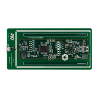
Top layer
The top layer (Figure 9) contains most of the components and PCB traces. The unused
areas around the ICs are filled with GND planes, guarded using via stitching. Furthermore,
important analog traces are surrounded by GND vias.
Mid layer 1
This layer (Figure 10) is a pure GND plane, providing a low ohmic DC path for the GND
connection.
Mid layer 2
Mid layer 2 (Figure 11) is used for the power distribution. It contains the power planes for the
5 V supply of the ST25R3911B and the 3.3 V supply of the microcontroller.
Bottom layer
The bottom layer (Figure 12) is mainly a GND plane, but some traces are routed through it.
 Loading...


