Hardware UM2042
6/25 DocID029132 Rev 3
2 Hardware
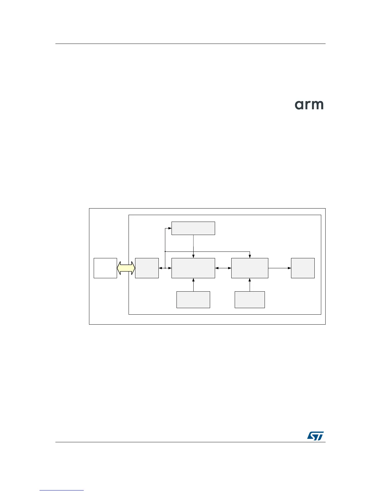
The PCB (Printed Circuit Board) is connected via USB to the PC. The STSW-ST25R001 PC
software controls the STM32 MCU located on the PCB. The STM32 MCU (based on Arm
®
core) then operates the ST25R3911B via SPI.
The ST25R3911B is connected directly to the 5 V supply of the USB bus. An LDO converts
this voltage down to 3.3 V, to supply the microcontroller.
A green LED close to the USB plug indicates if the bo
ard is powered. Six blue LEDs indicate
the mode of operation (transmit / receive) and which technologies are in use.
The antenna runs along the PCB perimeter.
2.1 Block diagram
Figure 2 shows the functional block diagram of the board.
Figure 2. Functional block diagram
2.2 Schematics
As indicated in Figure 3, the schematics can be split into four main parts
• USB con
nectivity and power supply (Figure 4)
• STM32 MCU (Figure 5)
• ST25R3911B (Figure 6)
• Antenna and matching network components (Figure 7)
 Loading...


