Reading/programming the embedded Flash memory PM0075
18/31 Doc ID 17863 Rev 1
● Pages 0-3 (for low- and medium-density devices), or pages 0-1 (for high-density and
connectivity line devices) are automatically write-protected. The rest of the memory can
be programmed by the code executed from the main Flash memory (for IAP, constant
storage, etc.), but it is protected against write/erase (but not against mass erase) in
debug mode or when booting from the embedded SRAM.
● All features linked to loading code into and executing code from the embedded SRAM
are still active (JTAG/SWD and boot from embedded SRAM) and this can be used to
disable the read protection. When the read protection option byte is altered to a
memory-unprotect value, a mass erase is performed.
● When booting from the embedded SRAM, Flash memory accesses through the code
and through data read using DMA1 and DMA2 are not allowed.
● Flash memory access through data read using JTAG, SWV (serial wire viewer),
SWD(serial wire debug), ETM and boundary scan are not allowed.
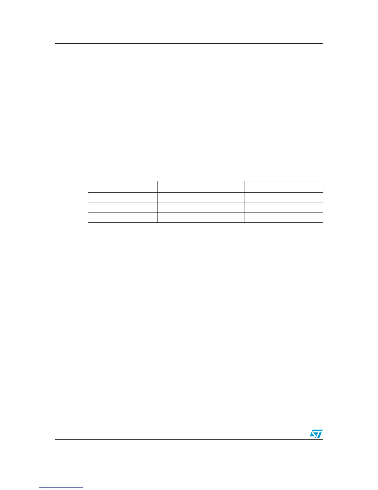
The Flash memory is protected when the RDP option byte and its complement contain the
pair of values shown in Tabl e 5.
Note: Erasing the option byte block will not trigger a mass erase as the erased value (0xFF)
corresponds to a protected value.
Unprotection
To disable the read protection from the embedded SRAM:
● Erase the entire option byte area. As a result, the read protection code (RDP) will be
0xFF. At this stage the read protection is still enabled.
● Program the correct RDP code 0x00A5 to unprotect the memory. This operation first
forces a Mass Erase of the main Flash memory.
● Reset the device (POR Reset) to reload the option bytes (and the new RDP code) and,
to disable the read protection.
Note: The read protection can be disabled using the boot loader (in this case only a System Reset
is necessary to reload the option bytes). For more details refer to AN2606.
2.4.2 Write protection
In high-density and connectivity line devices, from page 0 to page 61, write protection is
implemented with a granularity of two pages at a time. The remaining memory block (from
page 62 to page 255 in high-density devices, and from page 62 to page 127 in connectivity
line devices) is write-protected at once.
In low- and medium-density devices, write protection is implemented with a granularity of
four pages at a time.
If a program or an erase operation is performed on a protected page, the Flash memory
returns a protection error flag on the Flash memory Status Register (FLASH_SR).
Table 5. Flash memory protection status
RDP byte value RDP complement value Read protection status
0xFF 0xFF Protected
RDPRT Complement of RDP byte Not protected
Any value Not the complement value of RDP Protected
 Loading...