EasyManua.ls Logo

ST STM32F103xx series User Manual

ST STM32F103xx series
31 pages
To Next Page IconTo Next Page
To Previous Page IconTo Previous Page
Page #16 background imageLoading...
Page #16 background image
Reading/programming the embedded Flash memory PM0075
16/31 Doc ID 17863 Rev 1
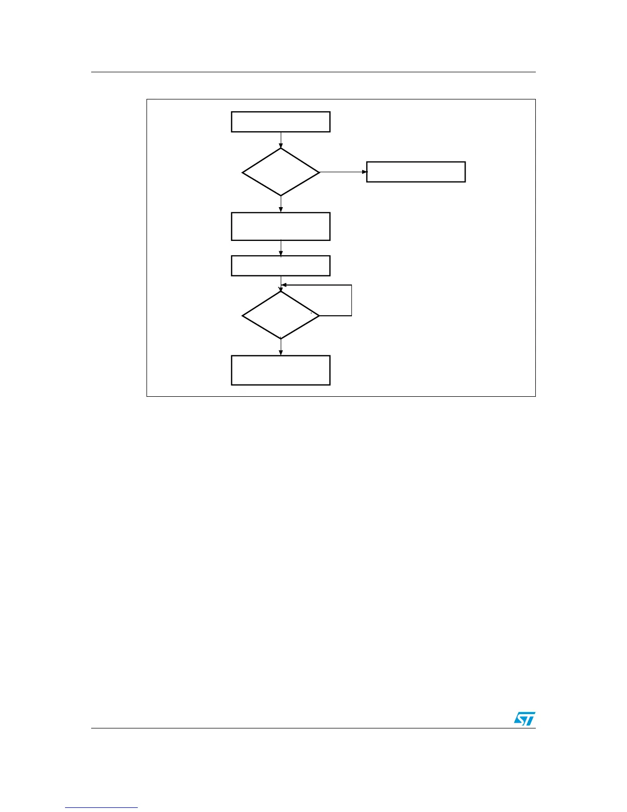
Figure 3. Flash memory Mass Erase procedure
2.3.5 Option byte programming
The option bytes are programmed differently from normal user addresses. The number of
option bytes is limited to 8 (4 for write protection, 1 for read protection, 1 for configuration
and 2 for user data storage). After unlocking the FPEC, the user has to authorize the
programming of the option bytes by writing the same set of KEYS (KEY1 and KEY2) to the
FLASH_OPTKEYR register to set the OPTWRE bit in the FLASH_CR register (refer to
Section 2.3.1 for key values). Then the user has to set the OPTPG bit in the FLASH_CR
register and perform a half-word write operation at the desired Flash address.
FPEC preliminarily reads the value of the addressed option byte and checks that it has been
erased. If not, the program operation is skipped and a warning is issued by the WRPRTERR
bit in the FLASH_SR register. The end of the program operation is indicated by the EOP bit
in the FLASH_SR register.
The FPEC takes the LSB and automatically computes the MSB (which is the complement of
the LSB) and starts the programming operation. This guarantees that the option byte and its
complement are always correct.
2EAD&,!3(?#2?,/#+
&,!3(?#2?,/#+

9E S
.O
9E S
.O
0ERFORMUNLOCKSEQUENCY
7RITEINTO&,!3(?#2?-%2
TO
7RITE&,!3(?#2?3424TO
&,!3(?32?"39

#HECKTHEERASEOPERATIONBY
READINGALLTHEADDRESSESIN
THEUSERMEMORY
AIB
Question and Answer IconNeed help?

Do you have a question about the ST STM32F103xx series and is the answer not in the manual?

ST STM32F103xx series Specifications

General IconGeneral
SeriesSTM32F103xx
CoreARM Cortex-M3
Operating FrequencyUp to 72 MHz
GPIO PinsUp to 80
Operating Voltage2.0 V to 3.6 V
ADC12-bit
Communication InterfacesUSART, SPI, I2C, CAN, USB
Operating Temperature-40°C to +85°C
PackageBGA

Summary

STM32F10xxx Flash Memory Programming and Erasing

Flash Memory Read Operations and Prefetching

Details how to read data from Flash memory, including instruction fetches and prefetch buffer.

Flash Program and Erase Controller (FPEC)

Covers the FPEC block, its registers, and key values for memory operations.

Unlocking Flash Memory and Main Programming

Explains the sequences for unlocking FPEC and the process of programming main Flash memory.

Flash Memory Erase Procedures

Details methods for erasing Flash memory, including page and mass erase operations.

STM32F10xxx Option Byte Programming

Describes the specific procedure for programming the device's option bytes.

Flash Memory Protection Mechanisms

Covers read protection, unprotection, and write protection for Flash memory.

STM32F10xxx Flash Interface Register Details

Related product manuals