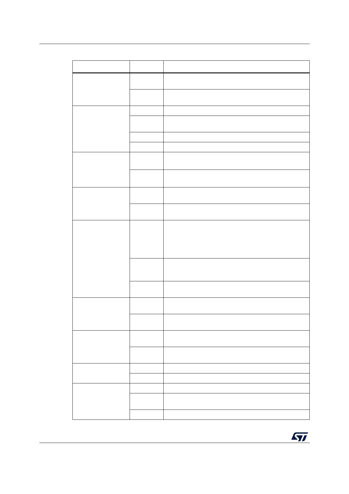
Hardware layout and configuration UM2407
30/49 UM2407 Rev 3
SB14 (SDMMC_D0),
SB15 (SDMMC_D1)
ON
These pins are connected to the ST morpho connector
(CN12).
OFF
These pins are disconnected from the ST morpho connector
(CN12) to avoid stubs of SDMMC data signals on the PCB.
SB39, SB47
(LD1-LED)
ON, OFF Green user LED (LD1) is connected to PB0.
OFF, ON
Green user LED (LD1) is connected to D13 of the
ARDUINO
®
signal (PA5).
OFF, OFF Green user LED (LD1) is not connected.
ON, ON Forbidden
SB33, SB35
(D11)
OFF, ON
D11 (pin 14 of CN7) is connected to STM32H7 PB5
(SPI_A_MOSI/ TIM_D_PWM2)
ON, OFF
D11 (pin 14 of CN7) is connected to STM32H7 PA7
(SPI_A_MOSI/ TIM_E_PWM1)
SB40, SB41
(X2 crystal)
OFF, OFF
PC14 and PC15 are not connected to the ST morpho
connector (CN11). X2 is used to generate the 32 kHz clock.
ON, ON
PC14 and PC15 are connected to the ST morpho connector
(CN11). R38 and R39 must be OFF.
SB44 (PF1/PH1)
SB46 (PF0/PH0)
(main clock)
ON, OFF
PF0/PH0 is not connected to the ST morpho connector
(CN11).
PF1/PH1 is connected to the ST morpho connector
(MCO is used as the main clock for STM32H7 on PF0/PH0–
SB45 ON).
OFF, OFF
PF0/PH0 and PF1/PH1 are not connected to the ST morpho
connector (CN11). X3, C69, C70, SB3, and SB4 provide a
clock. In this case, SB45 must be OFF.
ON, ON
PF0/PH0 and PF1/PH1 are connected to the ST morpho
connector (CN11). SB3, SB4, and SB45 must be OFF.
SB45
(STLK_MCO)
ON
MCO of ST-LINK (STM32F723IEK6) is connected to
PF0/PH0 of STM32H7.
OFF
MCO of ST-LINK (STM32F723IEK6) is not connected to
PF0/PH0 of STM32H7.
SB3, SB4
(external 25M crystal)
OFF, OFF
PF0/PH0 and PF1/PH1 are not connected to an external
25 MHz crystal X3.
ON, ON
PF0/PH0 and PF1/PH1 are connected to an external 25 MHz
crystal X3.
SB52
(V
BAT
)
ON V
BAT
pin of STM32H7 is connected to V
DD_MCU
.
OFF V
BAT
pin of STM32H7 is not connected to V
DD_MCU
.
SB51, SB58
(B1-USER)
ON, OFF B1 push-button is connected to PC13.
OFF, ON
B1 push-button is connected to PA0 (set SB51 OFF if the ST
Zio connector is used).
OFF, OFF B1 push-button is not connected.
Table 14. Solder bridge and jumper configuration (continued)
Bridge State
(1)
Description