42
X11SSV-Q User's Manual
SGPIO Header
The I-SGPIO1 (Serial General Purpose Input/Output) header is used to communicate with
the enclosure management chip on the backplane via the PCH SATA controller.
SGPIO Header
Pin Denitions
Pin# Denition Pin# Denition
1 NC 2 NC
3 Ground 4 DATA Out
5 Load 6 Ground
7 Clock 8 NC
NC = No Connection
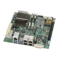
SINGLE-LINK
m-PCIE(F/H)
M.2
HD
AUDIO
CPU SLOT1 PCI-E 3.0 X16
PWR
LED
NICHDD
LED
NIC
21
OH/FF
USB11/12
USB7/8
RSTX
PWR
JF1
ON
(3.0)
USB5/6
USB9
COM1/2
DVI-I
DIMMA1
DIMMB1
UNB NON-ECC DDR4 DIMM REQUIRED
LAN2
USB3/4(3.0)
REV:
X11SSV-Q
1.01
USB1/2(3.0)
LAN1
CPU
DESIGNED IN USA
DP
HDMI
MAC CODE
BAR CODE
BIOS
LICENSE
A
C
1
JGPIO1
JI2C1
JI2C2
JWD1
JVR1
JPAC1
JPME2
JPUSB1
JSMB1
JD1
JL1
JSD1
JSD2
JTPM1
SRW6
SRW5
I-SATA0
I-SATA1
I-SATA4
I-SATA3
I-SATA2
SRW2
SRW1
JBT1
LED1
JF1
BT1
JPW1
JPW2
JP1
FAN4
FAN2
FAN3
FAN1
J3
I-SGPIO1
1
2
1. I-SGPIO1
2. JGPIO1
General Purpose I/O Header
JGPIO1 is a 10-pin general purpose I/O header located near PCI-E x16 slot. Each pin can
be congured to be an input pin or output pin in 2.54mm pitch. The GPIO is controlled via
the PCA9554 8-bit GPIO expansion from PCH SMBus. The base address is 0xF040(D31:F4).
Expander slave address is 0x70. Refer to the table below for pin denitions.
JGPIO Header
Pin Denitions
Pin# Denition Pin# Denition
1 +5V Power 2 Ground
3 GPIO0 4 GPIO1
5 GPIO2 6 GPIO3
7 GPIO5 8 GPIO5
9 GPIO6 10 GPIO7
I-SGPIO1 Header Pin Layout
JGPIO1 Header Pin Layout
9
 Loading...