M850-00
T856/857 Circuit Operation
C2.3
Copyright TEL 31/09/98
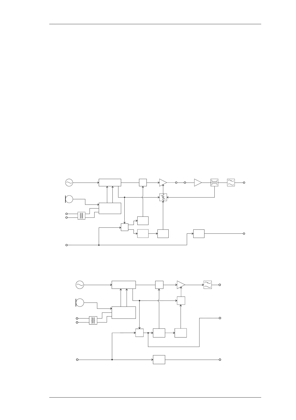
2.1 Introduction
The individual circuit blocks which make up the T856 and T857 are:
• synthesiser
•VCO
• audio processor
• drive amplifier
• power amplifier (T856 only)
• voltage regulators.
Each of these circuit blocks is set in its own shielded compartment, formed as an inte-
gral part of the main chassis.
The configuration of the circuit blocks may be seen on a functional level in Figure 2.1
and Figure 2.2. Refer to the circuit diagrams in Section 6.2 (T856) or 6.3 (T857) for more
detail.
Figure 2.1 T856 High Level Block Diagram
Figure 2.2 T857 High Level Block Diagram
Ramp
Gen.
Time
Delay
Time
Delay
Time
Delay
Audio
Processor
Synthesiser
+22dBm
Reference
Oscillator
12.8MHz
Microphone
Line
Transformer
Lock
Detect
PIN
Switch
Power
Control
Drive
Amp.
PA
VCO
Gate
Directional
Coupler
Low Pass
Filter
Exciter
Output
(+30dBm to
+33dBm)
Transmitter
Output
(25W)
Tx Reg
&
Audio
Processor
Synthesiser
+22dBm
Reference
Oscillator
12.8MHz
Microphone
Line
Transformer
Lock
Detect
PIN
Switch
Switching
Control
Drive
Amp.
Gate
Exciter
Output
(+28dBm to
+31dBm)
&
Ramp
Gen.
Tx Reg
VCO
Time
Delay
Time
Delay
Low Pass
Filter
PA Control Signal
(via exciter RF coax)
 Loading...


