D2.4
T858/859 Circuit Operation
M850-00
31/09/98 Copyright TEL
2.2 RF Circuitry
(Refer to the RF section circuit diagram in Section 5.)
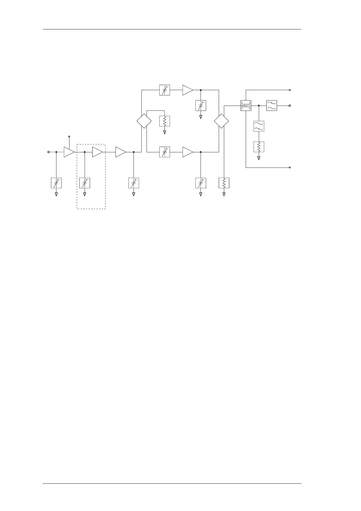
Figure 2.2 T858/859 RF Circuitry Block Diagram
The driver stage of the T858/859 consists of a three-stage transistor amplifier (Q1, Q3 &
Q4) which delivers 30W in the T858 and 50W in the T859. This signal is split via a 3dB
coupler (L19) and used to drive the two final amplifiers (Q6 & Q7). The outputs from
the finals are passed to the antenna socket via the harmonic filter.
The diplexer presents the final amplifiers with a good load at harmonic frequencies,
which helps to achieve the expected harmonic attenuation in the output filter.
The directional coupler senses forward and reflected power, which is rectified (D1 & D2)
and passed to the control circuitry for metering, alarm and power control purposes.
Power control is via a series pass transistor (Q16), which controls the supply voltage on
the collector of the driver transistor (Q1).
L19
L39
Q1 Q3 Q4 Q7
Q6
CV34
CV57
CV51
CV35
CV32CV8CV1
(T859
Only)
(T858 & T859
Only)
RF In
SK1
Power
Control
50Ω
Load
50Ω
Load
LPF
HPF
Load
Reverse
Power
RF Out
SK2
Forward
Power
 Loading...


