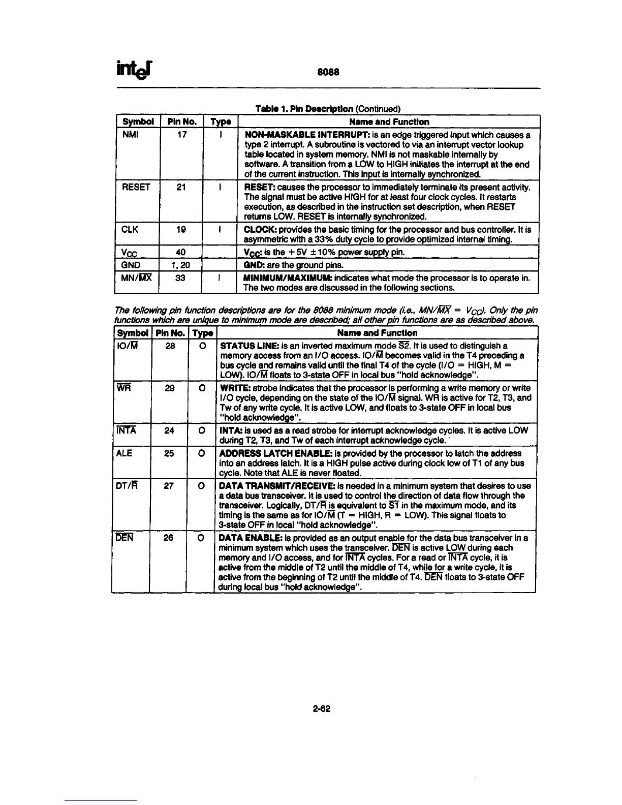
8088
Table
1.
Pin Description (Continued)
Symbol
NMI
RESET
CLK
Vcc
GND
MN/MX
Pin
No.
17
21
19
40
1,20
33
Type
I
I
I
I
Name and Function
NON-MASKABLE INTERRUPT: is an edge triggered input which causes a
type 2 interrupt. A subroutine is vectored to via an interrupt vector lookup
table located in system memory. NMI is not maskable internally by
software. A transition from a LOW to HIGH initiates the interrupt at the end
of the current
instruction.
This input is internally synchronized.
RESET: causes the processor to immediately terminate its present activity.
The signal must be active HIGH for at least four clock cycles. It restarts
execution,
as described in the instruction set
description,
when RESET
returns LOW. RESET is internally synchronized.
CLOCK: provides the basic timing for the processor and bus controller. It is
asymmetric with a
33%
duty cycle to provide optimized internal timing.
V
C
c-"
j
s the + 5V ±10% power supply pin.
QND:
are the ground pins.
MINIMUM/MAXIMUM: indicates what mode the processor is to operate in.
The two modes are discussed in the following sections.
The following pin function descriptions are for the 8088 minimum mode
(i.e.,
MN/MX = Vcc)- Only the pin
functions which are unique to minimum mode are
described;
all other pin functions are as described
above.
Symbol
lO/Ef
WR
IF3TA
ALE
DT/E
Pin
No.
28
29
24
25
27
26
Type
o
0
0
0
0
0
Name and Function
STATUS
LINE:
is an inverted maximum mode
§2.
It is used to distinguish a
memory access from an I/O access. IO/M becomes valid in the T4 preceding a
bus cycle and remains valid until the final T4 of the cycle (I/O = HIGH, M =
LOW). IO/M floats to
3-state
OFF in local bus "hold acknowledge".
WRITE:
strobe indicates that the processor is performing a write memory or write
I/O
cycle,
depending on the state of the IO/M signal. WR is active for
T2,
T3, and
Tw of any write cycle. It is active LOW, and floats to
3-state
OFF in local bus
"hold acknowledge".
INTA: is used as a read strobe for interrupt acknowledge cycles. It is active LOW
during
T2,
T3, and Tw of each interrupt acknowledge cycle.
ADDRESS LATCH
ENABLE:
is provided by the processor to latch the address
into an address
latch.
It is a HIGH pulse active during clock low of
T1
of any bus
cycle.
Note that ALE is never floated.
DATA TRANSMIT/RECEIVE: is needed in a minimum system that desires to use
a data bus transceiver. It is used to control the direction of data flow through the
transceiver. Logically, DT/ft is equivalent to ST in the maximum mode, and its
timing is the same as for IO/M (T = HIGH, R = LOW). This signal floats to
3-state
OFF in local "hold acknowledge".
DATA ENABLE: is provided as an output enable for the data bus transceiver in a
minimum system which uses the transceiver. DEN is active LOW during each
memory and I/O access, and for INTA cycles. For a read or INTA cycle, it is
active from the middle of T2 until the middle of
T4,
while for a write cycle, it is
active from the beginning of T2 until the middle of
T4.
DEN floats to
3-state
OFF
during local bus "hold acknowledge".
2-62
 Loading...