Theory of Operation— 2213 Service
SI 05
R138
CH 1
VERT
SIC
TO
PREAMP
STEP BAL
HIGH-Z ATTENUATOR
VOLTS/
DIV
+ 1 +10 + 100
2 mV
X
5 mV
X
10 mV
X
20 mV
X
50 mV
X
100 mV
X
200 mV
X
500 mV
X
1 V X
2 V X
5 V X
10 V X
LOV-Z ATTENUATOR
VOLTS/
DIV
+ 1 + 2.5
+ 5
2 mV
X
5 mV
X
10 mV
X
20 mV
X
50 mV
X
100 mV
X
200 mV
X
500 mV
X
1 V
X
2 V
X
5 V X
10 V X
X1/X10 AMPL
VOLTS/
DIV
XI X10
2 mV X
5 mV X
10 mV X
20 mV
X
50 mV X
100 mV X
200 mV X
500 mV
X
1 V X
2 V
X
5 V X
10 V X
3826-21
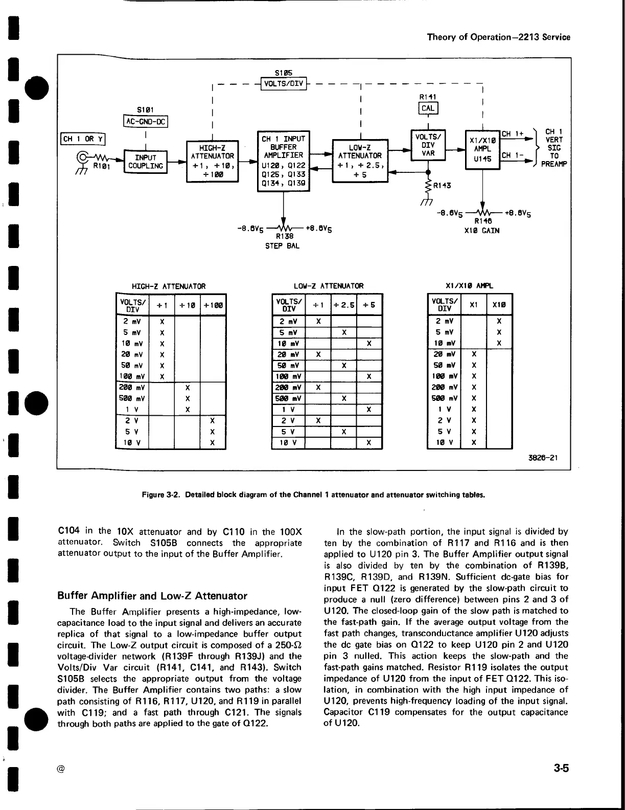
Figure 3-2. Detailed block diagram of the Channel 1 attenuator and attenuator switching tables.
C104 in the 10X attenuator and by Cl 10 in the 100X
attenuator. Switch S105B connects the appropriate
attenuator output to the input of the Buffer Amplifier.
Buffer Amplifier and Low-Z Attenuator
The Buffer Amplifier presents a high-impedance, low-
capacitance load to the input signal and delivers an accurate
replica of that signal to a low-impedance buffer output
circuit. The Low-Z output circuit is composed of a 250-12
voltage-divider network (R139F through R139J) and the
Volts/Div Var circuit (R141, C141, and R143). Switch
S105B selects the appropriate output from the voltage
divider. The Buffer Amplifier contains two paths: a slow
path consisting of R116, R117, U120, and R119 in parallel
with Cl 19; and a fast path through C121. The signals
through both paths are applied to the gate of Q122.
In the slow-path portion, the input signal is divided by
ten by the combination of R117 and R116 and is then
applied to U120 pin 3. The Buffer Amplifier output signal
is also divided by ten by the combination of R139B,
R139C, R139D, and R139N. Sufficient dc-gate bias for
input FET Q122 is generated by the slow-path circuit to
produce a null (zero difference) between pins 2 and 3 of
U120. The closed-loop gain of the slow path is matched to
the fast-path gain. If the average output voltage from the
fast path changes, transconductance amplifier U120 adjusts
the dc gate bias on Q122 to keep U120 pin 2 and U120
pin 3 nulled. This action keeps the slow-path and the
fast-path gains matched. Resistor R119 isolates the output
impedance of U120 from the input of FET Q122. This iso
lation, in combination with the high input impedance of
U120, prevents high-frequency loading of the input signal.
Capacitor Cl 19 compensates for the output capacitance
of U120.
3-5
 Loading...


