CIRCUIT DESCRIPTION
Section 3-485/R485 Service
Introduction
This section describes the electrical operation and
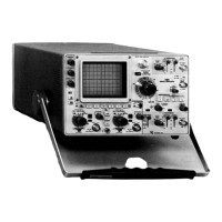
relationship of the circuits in the Type 485. The theory of
operation for circuits that are used only in this instrument
are described in detail in this discussion. Circuits that are
commonly used in the electronics industry are not
described in detail.
50 ft ATTENUATOR
Two identical attenuators, one for each vertical channel,
are used to select the desired vertical sensitivity of the 485.
Each attenuator is an integral unit containing various 50 ft
attenuators, input overload protection circuitry and, where
applicable, a 1 megohm attenuator and 1 megohm buffer
amplifier.
The 50 ft attenuator is comprised of a delay line,
DL410, and four 50 ft attenuator sections. The -f 2 and -r
2.5 50 ft attenuator sections are shared by a 1 Mft buffer
amplifier. The two t 10 attenuator sections are used only in
the 50 ft mode. The delay line equalizes the delay
differences between the 1 M ft buffer amplifier and the
50 ft mode. R127 provides termination for the 1 M ft
buffer amplifier when the instrument is operating in the
50 ft mode.
1 MEGOHM BUFFER AMPLIFIER
The 1 megohm buffer amplifier provides a high input
impedance and unity gain when terminated in 50 ft. It is
connected to the input through relay K1S1 only in the 1
megohm mode and when the RESET light is on.
C33 and R33 provide input current limiting. CR33
clamps negative transients in excess of 9.6 V to protect
FET Q34. The gate to drain junction of Q34 gives clamping
for positive-going overloads. The high frequency signal path
goes from the input FET to Q40, an emitter follower. R53
sets the high frequency gain. Q60 drives Q62; CR62
balances out the base-emitter voltage of Q62 and temper
ature compensates it to keep the standing current in Q62
independent of temperature. Q62 current drives the output
for positive signal swings. Q60 also drives Q70, which pulls
the output negative through R69 and serves as reverse
termination at high frequencies. CR64 and CR65 work as
expanders for high amplitude signals. R55 and C55 are high
frequency adjustments which affect the first five nano
seconds of the transient response. L56 and L71 are integral
parts of the circuit board providing high frequency peaking.
Q50 is a low impedance drive for the low frequency
feedback path.
Low frequency feedback is accomplished by U48, which
compares the voltage levels at the base of Q40 and the
output, J70. C46 matches the time constant of C77 and
R75 with the time constant of R42 and parallel combina
tion of C46 and C47. C48 sets the bandwidth of U48.
50 ft OVERLOAD PROTECTION
In the 50 ft mode, K1 is closed by U80, which routes
the signal to the 50 ft attenuator. 50 ft input protection is
provided by an RMS detecting circuit in U80. R84 and
R107 attenuate the input signal 100X for U80. C86, C87,
and R87 integrate a signal proportional to the RMS value of
the signal at pin 3 of U80. When an overload is detected,
K1 is de-energized, removing the signal from the 50 ft
attenuator section and applying it to the input of the 1
megohm buffer amplifier. U80 also lights DS96, the RESET
light. To reset, S125B is switched to the 1 megohm
position, causing the scope to be in the 1 megohm mode.
Return to the 50 ft mode is then accomplished by pushing
SI258 (50 ft/1 megohm mode switch) again.
VERTICAL PREAMPLIFIER
CH 2 is identical to CH 1 except that CH 2 has a polarity
switch. Only CH 2 will be described here. The CH 2 signal is
received from the CH 2 attenuator through J300. Diode
bridge CR301, CR302, CR303, and CR304 protects the
input from large signals that occur too fast for the input
protection relay to react. T305 is a balun, providing a
push-pull signal to U310 at high frequencies. The 50 ft
input termination consists of R308, R305, and R309. R308
is adjusted to give 50 ft DC resistance at input connector
J1. CH 2 offset control R306 adjusts the voltage at the
input connector J1 to zero in the absence of an input
signal. Either R310 or R312 is selected by the POLARITY
switch S310, allowing the variable control to be balanced in
both invert and normal modes. The output leads of U310
(pins 5, 6, 8, and 9) are crossed over so that the polarity of
the signal can be inverted. R90, the variable control, and
the resistor network R317, R319, R325, R326, R327, and
R328 determine the ratio of currents in pin 11 and pin 12,
hence the ratio of currents in transistors connected to pins
6 and 8 to the current in transistors connected to pins 5
and 9. Varying this ratio controls the gain of U3101. At all
sensitivities other than 5mV/div, pins 11 and 12 of U350
are shorted together by S95. Thus half the signal current in
U350 is lost through R367 and R368. In 5 mV/div, S95
contacts open, causing all of the signal current to flow in
the transistors connected to pins 5 and 9, doubling the gain
'Gilbert, Barrie, A New Wide-Band Amplifier Technique, IEEE
Journal of Solid State Circuits, Vot SC-3 number 4, December,
1968, P353.
®
3-1

 Loading...