Maintenance—492/492P Service Vol. 1 (SN B030000 & up)
If the test completes successfully, the microcomputer
pulses repeatedly the OK LED, DS1032, to indicate the
number of empty memory blocks found. The LED blinks
N + 1 times, where N is the number of empty ROM sockets
(the memory block 1600—1800 is not used). If the GPIB
board is not installed, its eight ROM sockets are counted as
empty. If the LED blinks more than N + 1 times, a ROM (or
ROMs) failed to respond in Step 3; look for a possible prob
lem on the chip-select line or on the MSB (bit 7) data line.
If the microcomputer seems to test ok, but does not con
trol the instrument, skip to the Instrument Bus Check,
where microcomputer communication with the rest of the
instrument is exercised.
Microcomputer Test Mode
A microcomputer test mode is selected by moving jump
er P1020 on the Processor board to the TEST position. This
hardwires the 6800 data lines to hex 5F. As a result, the
6800 continuously executes a CLRB instruction, repetitively
cycling through all of its address space. The instrument
does not function in this mode. Rather it sets up a known
pattern on the microcomputer address, data, and control
lines and at the output of address decoders. This mode al
lows an attack on problems that prevent the microcomputer
from running its self-test check.
NOTE
If CR2025 on the Processor board is missing, it may
be added as shown on the Processor diagram to
make the correct instruction on the data lines.
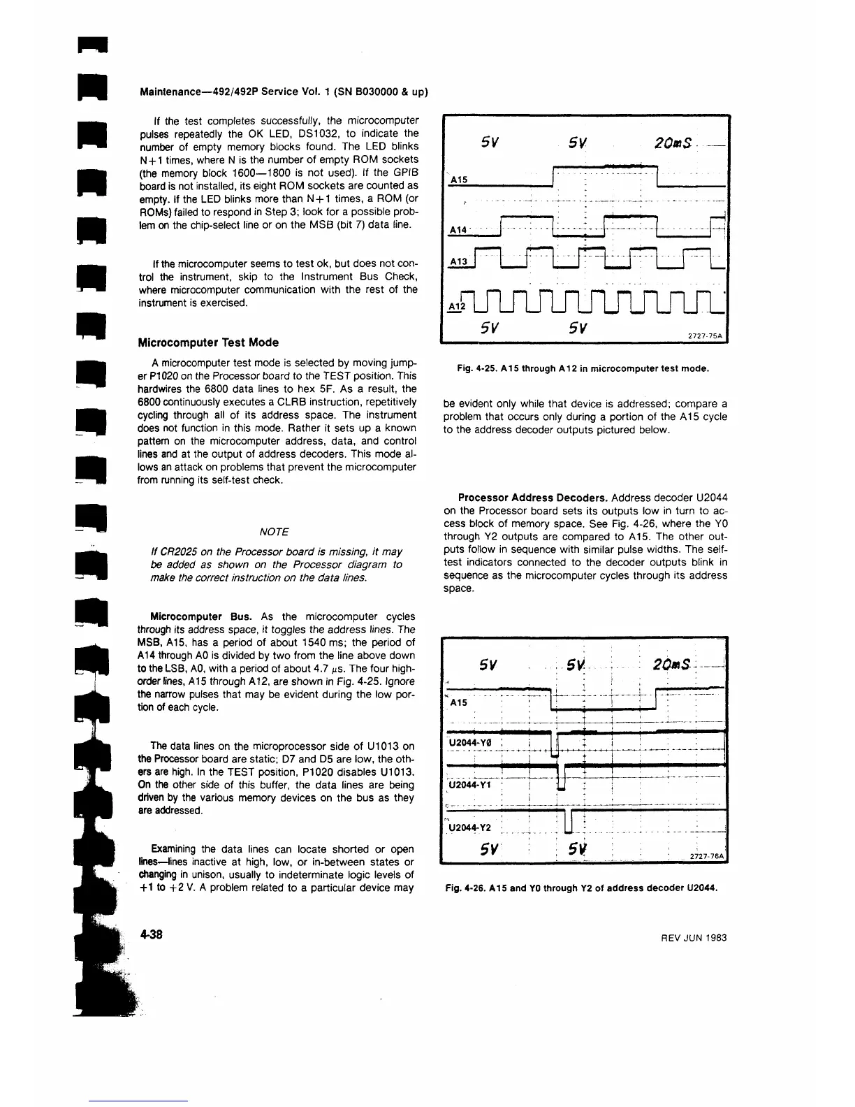
Microcomputer Bus. As the microcomputer cycles
through its address space, it toggles the address lines. The
MSB, A15, has a period of about 1540 ms; the period of
A14 through A0 is divided by two from the line above down
to the LSB, A0, with a period of about 4.7 με. The four high-
order lines, A15 through A12, are shown in Fig. 4-25. Ignore
the narrow pulses that may be evident during the low por
tion of each cycle.
The data lines on the microprocessor side of U1013 on
the Processor board are static; D7 and D5 are low, the oth
ers are high. In the TEST position, P1020 disables U1013.
On the other side of this buffer, the data lines are being
driven by the various memory devices on the bus as they
are addressed.
Examining the data lines can locate shorted or open
lines—lines inactive at high, low, or in-between states or
changing in unison, usually to indeterminate logic levels of
+1 to +2 V. A problem related to a particular device may
4-38
5V
5V 20mS —
A15
-
- · . . - 1 — · Z
------------
---
-------------
1 — - · - *
.................
...
-
A14
....
:
.....
..................
- I -
A13 I I |
^a^njuuinrum'
5V
5V
2727-75A
Fig. 4-25. A15 through A12 in microcomputer test mode.
be evident only while that device is addressed; compare a
problem that occurs only during a portion of the A15 cycle
to the address decoder outputs pictured below.
Processor Address Decoders. Address decoder U2044
on the Processor board sets its outputs low in turn to ac
cess block of memory space. See Fig. 4-26, where the Y0
through Y2 outputs are compared to A15. The other out
puts follow in sequence with similar pulse widths. The self
test indicators connected to the decoder outputs blink in
sequence as the microcomputer cycles through its address
space.
SV
SV 2 0 » S
----
1
A15
....—
I ! !
I
• t i : .
U2O44-Y0
i
*
i + i : ;
H*" t " j ;
i !
-----
-
U2044-Y1
Γ t
i ;
- \
U2044-Y2
SV
----
:
...................
.
SV
l : 2*
7 2 7- 7 6A
Fig. 4-26. A15 and Y0 through Y2 of address decoder U2044.
REV JUN 1983
 Loading...