Maintenance—492/492P Service Vol. 1 (SN B030000 & up)
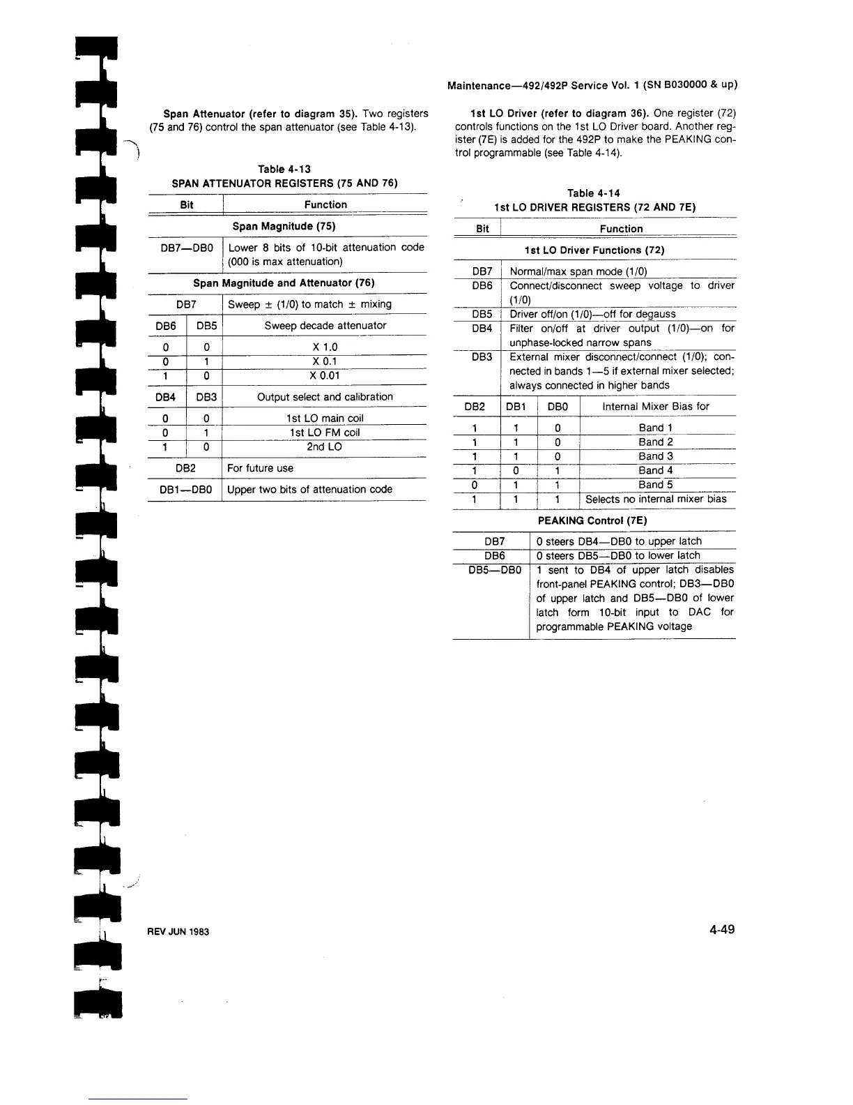
Span Attenuator (refer to diagram 35). Two registers
(75 and 76) control the span attenuator (see Table 4-13).
Table 4-13
SPAN ATTENUATOR REGISTERS (75 AND 76)
Bit
Function
Span Magnitude (75)
DB7—DBO
Lower 8 bits of 10-bit attenuation code
(000 is max attenuation)
Span Magnitude and Attenuator (76)
DB7
Sweep ± (1/0) to match ± mixing
DB6
DB5
Sweep decade attenuator
0
0 X 1.0
0
1 X 0.1
1 0
X 0.01
DB4 DB3
Output select and calibration
0
0
1 st LO main coil
0
1
1st LO FM coil
1 0
2nd LO
DB2 For future use
DB1—DBO
Upper two bits of attenuation code
1st LO Driver (refer to diagram 36). One register (72)
controls functions on the 1st LO Driver board. Another reg
ister (7E) is added for the 492P to make the PEAKING con
trol programmable (see Table 4-14).
Table 4-14
1st LO DRIVER REGISTERS (72 AND 7E)
Bit
Function
1st LO Driver Functions (72)
DB7 Normal/max span mode (1/0)
DB6
Connect/disconnect sweep voltage to driver
(1/0)
DB5
Driver off/on (1/0)—off for degauss
DB4 Filter on/off at driver output (1/0)—on for
unphase-locked narrow spans
DB3
External mixer disconnect/connect (1/0); con
nected in bands 1—5 if external mixer selected;
always connected in higher bands
DB2
DB1
DBO
Internal Mixer Bias for
1
1
0
Band 1
1
1
0
Band 2
1
1
0
Band 3
1 0 1
Band 4
0
1 1
Band 5
1 1 1
Selects no internal mixer bias
PEAKING Control (7E)
DB7 0 steers DB4—DBO to upper latch
DB6
0 steers DB5—DBO to lower latch
DB5—DBO
1 sent to DB4 of upper latch disables
front-panel PEAKING control; DB3—DBO
of upper latch and DB5—DBO of lower
latch form 10-bit input to DAC for
programmable PEAKING voltage
 Loading...