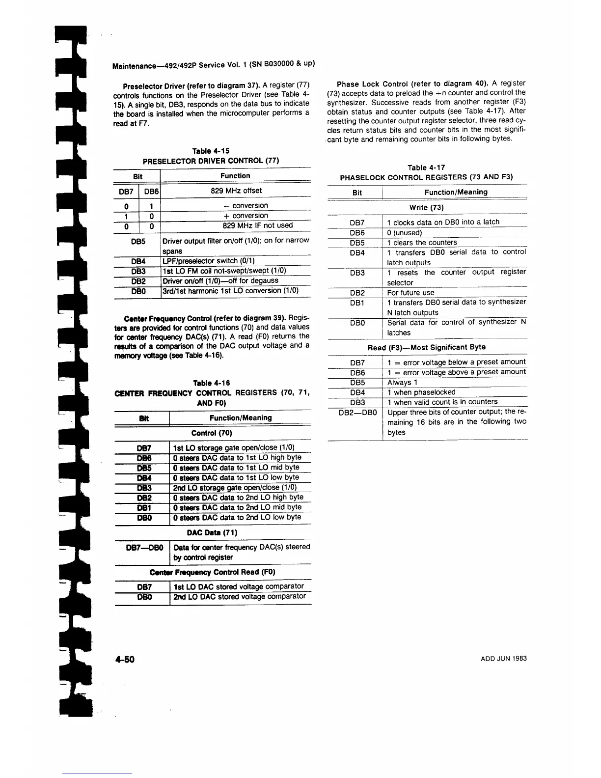
Maintenance— 492/492P Service Vol. 1 (SN B030000 & up)
Preselector Driver (refer to diagram 37). A register (77)
controls functions on the Preselector Driver (see Table 4
15). A single bit, DB3, responds on the data bus to indicate
the board is installed when the microcomputer performs a
read at F7.
Table 4-15
PRESELECTOR DRIVER CONTROL (77)
Bit
Function
DB7 DB6
829 MHz offset
0
1
— conversion
1
0
+ conversion
0
0
829 MHz IF not used
DB5
Driver output filter on/off (1/0); on for narrow
spans
DB4
LPF/preselector switch (0/1)
DB3
1st LO FM coil not-swept/swept (1/0)
DB2
Driver on/off (1/0)—off for degauss
DBO
3rd/1st harmonic 1st LO conversion (1/0)
Center Frequency Control (refer to diagram 39). Regis
ters are provided for control functions (70) and data values
for center frequency DAC(s) (71). A read (F0) returns the
results of a comparison of the DAC output voltage and a
memory voltage (see Table 4-16).
Table 4-16
CENTER FREQUENCY CONTROL REGISTERS (70, 71,
AND F0)
Bit
Function/Meaning
Control (70)
DB7
1st LO storage gate open/close (1/0)
DB6
0 steers DAC data to 1 st LO high byte
DB5
0 steers DAC data to 1 st LO mid byte
DB4
0 steers DAC data to 1st LO low byte
DB3
2nd LO storage gate open/close (1/0)
DB2
0 steers DAC data to 2nd LO high byte
DB1
0 steers DAC data to 2nd LO mid byte
DBO
0 steers DAC data to 2nd LO low byte
DAC Data (71)
DB7—DBO
Data for center frequency DAC(s) steered
by control register
Center Frequency Control Read (F0)
DB7
1st LO DAC stored voltage comparator
DBO
2nd LO DAC stored voltage comparator
Phase Lock Control (refer to diagram 40). A register
(73) accepts data to preload the n-n counter and control the
synthesizer. Successive reads from another register (F3)
obtain status and counter outputs (see Table 4-17). After
resetting the counter output register selector, three read cy
cles return status bits and counter bits in the most signifi
cant byte and remaining counter bits in following bytes.
Table 4-17
PHASELOCK CONTROL REGISTERS (73 AND F3)
Bit
Function/Meaning
Write (73)
DB7
1 clocks data on DBO into a latch
DB6
0 (unused)
DB5
1 clears the counters
DB4
1 transfers DBO serial data to control
latch outputs
DB3
1 resets the counter output register
selector
DB2
For future use
DB1
1 transfers DBO serial data to synthesizer
N latch outputs
DBO
Serial data for control of synthesizer N
latches
Read (F3)—Most Significant Byte
DB7
1 = error voltage below a preset amount
DB6
1 = error voltage above a preset amount
DB5
Always 1
DB4
1 when phaselocked
DB3
1 when valid count is in counters
DB2—DBO
Upper three bits of counter output; the re
maining 16 bits are in the following two
bytes
4-50
ADD JUN 1983
 Loading...