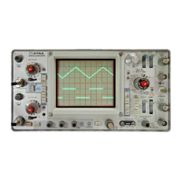
Theory of Operation—492/492P Service Vol. 1 (SN B030000 & up)
829 MHz enters the mixer diodes through a 450 MHz
highpass filter. The lowpass filter blocks the lower IF signals
generated within the mixer. The mixer diodes are transform-
er-driven with 719 MHz local oscillator. The large amplitude
LO signal (+12 dBm) drives the diodes into and out of con
duction, effectively switching the smaller 829 MHz signal on
and off at a 719 MHz rate. Several mixing products result,
the largest of which are the difference frequencies,
(110 MHz) and the sum (1548 MHz). The 110 MHz product
is allowed to leave the mixer by way of a 300 MHz lowpass
filter that blocks LO, RF, and higher frequency products.
The 1548 MHz product leaves the mixer via the 450 MHz
lowpass beyond which it is reflected by the 829 MHz
bandpass filter and returned to the mixer in-phase with LO
harmonics to increase energy of the 110 MHz signal. A
printed delay line between the 829 MHz bandpass and
1.3 GHz lowpass filters control the phase delay. The net
result of this “image enhancement” is low conversion loss
and good inter-modulation distortion performance. Inclusion
of the 3 dB attenuator reduces the image enhancement ef
fect considerably but allows line lengths and filter character
istics to be non-critical. Overall conversion loss from
829 MHz to 110 MHz is about 8.5 dB, including 2 dB from
the 829 MHz bandpass filter and 3 dB from the attenuator.
When the IF SELECT signal input is high, amplifier
Q1011 is turned on and shunt diode switches CR2012,
CR2013, and CR1015 turn off. This allows the 110 MHz IF
signal from the 2072 MHz 2nd Converter to be applied to
the output port. Series diode switch CR2011 also turns off
to prevent signal loss into the inactive 829 MHz 2nd Con
verter. Isolation for the 829 MHz 2nd Converter is not criti
cal when that converter is inactive, because the 719 MHz
local oscillator is also turned off by the IF SELECT signal.
This eliminates most spurious outputs. The switch and am
plifier logic is summarized in Table 5-3.
As described above, diodes are used as the basic switch
elements. When forward biased, with current of several
milliamps, the diodes present only a few ohms of series re
sistance to RF signals. When reverse biased, the diodes
present essentially an open circuit. The control signal from
switch driver Q2015 is connected in a series path through
the four diodes (CR2011, CR2012, CR2013, and CR1015)
and inductors L2011, L2013, and L2019 so that Q2015 sup
plies only a small current to forward bias all four diodes.
This same diode bias current is used to turn off amplifier
Q1011.
110 MHz IF Select Circuits
The 110 MHz IF Select circuits select the 110 MHz IF
signal from either the 829 MHz 2nd Converter or the
2072 MHz 2nd Converter for transmission to the 110 MHz
IF Amplifier. The 110 MHz IF signal from the 829 MHz Con
verter is applied directly to the select switch circuit; the
110 MHz IF signal from the 2072 MHz converter is applied
(via coaxial connector P233) through a controlled amplifier
to the select switch circuit. The switch circuit diodes are
CR2011, CR2012, CR2013, and CR1015.
Diodes CR2012 and CR2013 are incorporated into a pi-
type matching network consisting of inductors L2011,
L2013, and capacitor C2012 so that both switches shunt
the signal at moderately high impedance points. In addition,
when the switch diodes are turned on, parallel resonance,
between inductor L2011 and capacitor C2012, presents vir
tually an open circuit to signals passed by switch diode
CR2011. Switch diode CR2013 is located at the high imped
ance node created by series resonant inductor L2019 and
capacitor C2017. Diode CR1015 directly shunts the output
from amplifier 01011.
When the IF SELECT signal input to the 829 MHz 2nd
Converter (via feedthrough C236) is low, series diode switch
CR2011 turns on, allowing the 110 MHz IF signal, from the
829 MHz 2nd Converter, to be applied to the output port. At
the same time, shunt diode switches CR2012, CR2013, and
CR1015 turn on. Amplifier Q1011 turns off, thus isolating
the output port from spurious 2072 MHz 2nd Converter out
put signals.
Transistor Q1011 operates as a common-emitter amplifi
er for the 110 MHz IF signal from the 2072 MHz 2nd Con
verter. Its gain and impedance match are controlled
primarily by feedback resistors R1011 and R1012. Resis
tors R1013 and R1018 attenuate the output by approxi
mately 6 dB for enhanced control of match and stability
characteristics. Dc collector current from 01011 develops a
voltage across resistor R1017. Bias control transistor
Table 5-3
SWITCH AND AMPLIFIER SELECTION SUMMARY
IF Select
Series
Shunt
110-MHz
Line Switch
Switch Amplifier
IF Source
High
On
On
Off
829 MHz 2nd Conv.
Low
Off
Off On
2072 MHz 2nd Conv.
5-16 REV AUG 1981
 Loading...