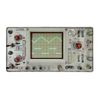
Theory of Operation—492/492P Service Vol. 1 (SN B030000 & up)
Q1012 then compares this voltage with the fixed voltage of
the divider, consisting of resistors R1015 and R1016. Any
variation in the Q1011 collector current is thus sensed by
Q1012 and cancelled by a resulting change in the Q1011
base current. Collector current in Q1011 is fixed in this man
ner at approximately 15 mA.
When control current is drawn through the switching di
odes by driver Q2015, a voltage is developed across resis
tor R1017 that exceeds the control limits of Q1012,
effectively removing the base bias from amplifier Q1011 and
turning off that transistor. Negative current supplied through
resistor R1014 ensures that Q1011 can be turned off by the
loss of positive base drive. Diode CR1011 protects the base
of Q1011 from excessive reverse bias. Voltage across
R1017 is approximately 3.4 V when Q1011 is turned on and
approximately 4.4 V when it is turned off. Overall gain for
the 110 MHz path is approximately 12.8 dB when the ampli
fier is turned on.
From the diode switch circuit, the 110 MHz IF signal is
transmitted via coaxial connector P232 to the 110 MHz IF
Amplifier.
829 MHz, 2nd Converter, LO Section
Refer to the block diagram adjacent to Diagram 14. The
829 MHz 2nd Converter Local Oscillator provides the
719 MHz frequency that is mixed with the 829 MHz IF sig
nal to produce the 110 MHz IF signal that is supplied to the
3rd Converter. (In the following description, the circuits are
referred to as the 719 MHz LO.) The 719 MHz LO consists
of a phaselock loop, a 719 MHz output circuit, and a 2nd LO
front panel output circuit. Refer to Diagram 14 while reading
the following description.
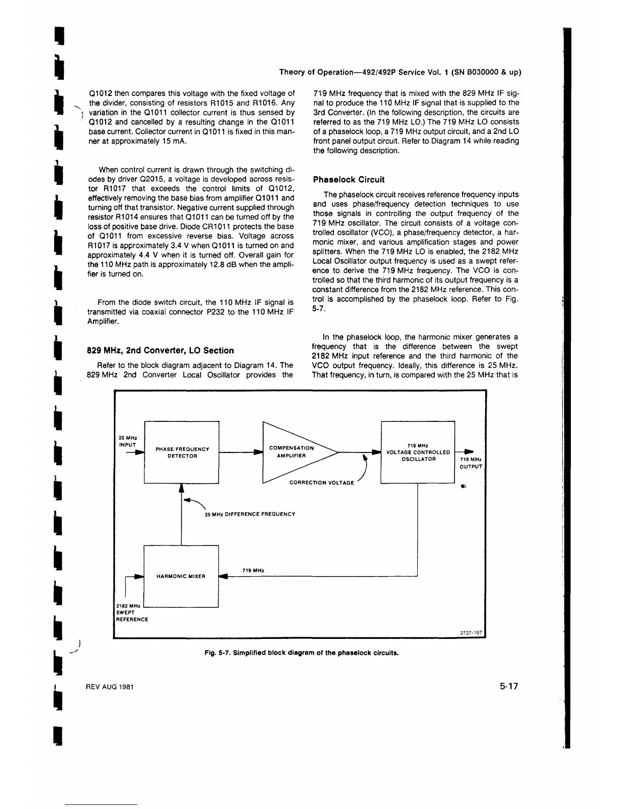
Phaselock Circuit
The phaselock circuit receives reference frequency inputs
and uses phase/frequency detection techniques to use
those signals in controlling the output frequency of the
719 MHz oscillator. The circuit consists of a voltage con
trolled oscillator (VCO), a phase/frequency detector, a har
monic mixer, and various amplification stages and power
splitters. When the 719 MHz LO is enabled, the 2182 MHz
Local Oscillator output frequency is used as a swept refer
ence to derive the 719 MHz frequency. The VCO is con
trolled so that the third harmonic of its output frequency is a
constant difference from the 2182 MHz reference. This con
trol is accomplished by the phaselock loop. Refer to Fig.
5-7.
In the phaselock loop, the harmonic mixer generates a
frequency that is the difference between the swept
2182 MHz input reference and the third harmonic of the
VCO output frequency. Ideally, this difference is 25 MHz.
That frequency, in turn, is compared with the 25 MHz that is
SWEPT
REFERENCE
Fig. 5-7. Simplified block diagram of the phaselock circuits.
REV AUG 1981 5-17
 Loading...