m m m - m
Theory of Operation—492/492P Service Vol. 1 (SN B030000 & up)
the amount of negative feedback decreases. Each diode in
the array is biased to conduct at successive amplitude
points, until all are conducting. As each diode conducts,
more current is drawn from the feedback loop which in
creases the gain of the amplifier. The resultant output volt
age is a non-linear function of the input of the +15 to
+40 V range. This voltage is applied to the varactor diode
port (Vv) to tune and sweep the oscillator.
Cavity Oscillator
Refer to the Cavity 2nd LO description in the 2nd Con
verter section.
To circumvent this problem, the outputs of the tandem
DAC units are summed together so that the two units are
overlapped by three bits (that is, the MSB of the low-order
DAC is weighted equally with the third least significant bit,
or 2E-10 bit). The overlap means that the lower DAC will
have sufficient range to monotonically tune the output of the
converter over the entire range of the analyzer, but only if
the proper codes of the lower DAC device can be found.
Now, suppose that the tandem DAC is loaded as follows:
Upper order:
100000000000
Lower order: 1111111111111
CENTER FREQUENCY CONTROL
Refer to the block diagram adjacent to Diagram 39. The
Center Frequency Control circuits form the electrical inter
face between the front-panel controls and the converter
stages in the 492/492P. The circuit receives digital informa
tion and instructions from the microcomputer, and converts
it to a coarse and fine tuning voltage that is applied to the
other elements of the Frequency Control system.
The Center Frequency Control circuits consist of the fol
lowing major blocks:
1) the Digital Control circuit, which buffers and decodes the
addresses and other data to control the other circuits;
2 ) the coarse and fine storage registers (latches), which
store the numerical bytes that control the DAC (digital-to-
analog converter) stages;
3) the coarse and fine DAC stages, which convert the digi
tal inputs from the storage registers into analog current and
voltage equivalent values;
4) the coarse and fine track/hold amplifiers, which store the
analog output values during the approximation routine, and
compare the stored value and the approximated value for
the microcomputer;
5) the write-back circuits, which inform the microcomputer
when the stored value and the approximated values are
equal.
Operating Modes
Some explanation of the design principles of the circuit is
required before the operation of the circuit can be dis
cussed. DAC devices are now available that can furnish the
resolution required to tune the analyzer in small enough
steps. To achieve the necessary amount of resolution, two
DAC devices are used in tandem. However, this method can
cause some errors and non-monotonic behavior in the over
all converter circuit.
The contents of the devices are shown overlapped to
illustrate the bit weighting. Now assume that the low-order
device is to be incremented one bit. The MSB of the low-
order device must be moved into the high-order device be
fore the low-order device can be incremented. Thus, the two
must appear as shown below:
High-order:
100000000100
Low-order: 011111111111
If the high-order device operated with no overall linearity
inaccuracy, the operation would now be complete, and the
low-order incrementation could occur. However, the DAC
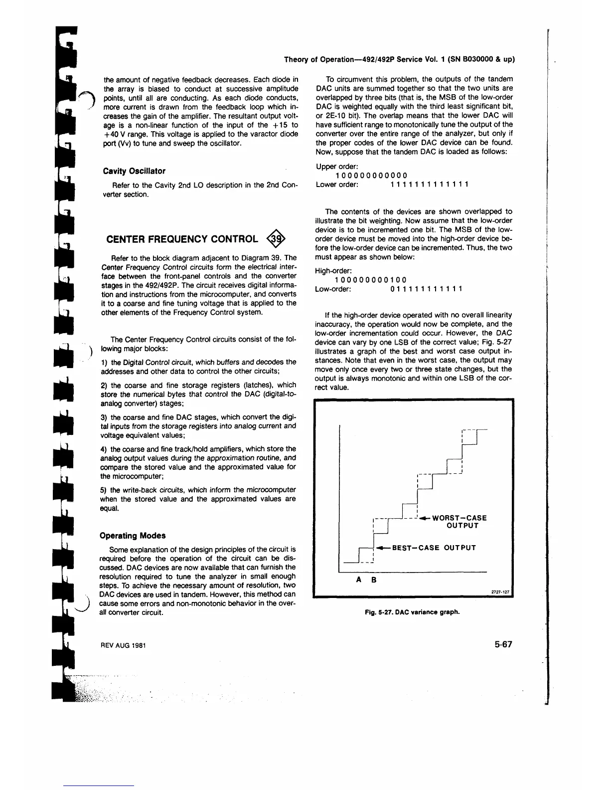
device can vary by one LSB of the correct value; Fig. 5-27
illustrates a graph of the best and worst case output in
stances. Note that even in the worst case, the output may
move only once every two or three state changes, but the
output is always monotonic and within one LSB of the cor
rect value.
Fig. 5-27. DAC variance graph.
REV AUG 1981
5-67


 To Next Page
 Loading...