Theory of Operation—492/492P Service Vol. 1 (SN B030000 & up)
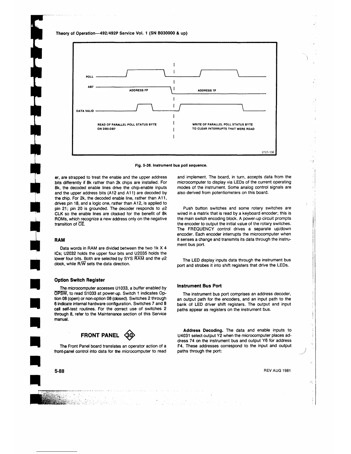
ADDRESS FF
DATA VALID
READ OF PARALLEL POLL STATUS BYTE
ON DB0-DB7
ADDRESS 7F
WRITE OF PARALLEL POLL STATUS BYTE
TO CLEAR INTERRUPTS THAT WERE READ
2727-136
Fig. 5-36. Instrument bus poll sequence.
er, are strapped to treat the enable and the upper address
bits differently if 8 k rather than 2k chips are installed. For
8 k, the decoded enable lines drive the chip-enable inputs
and the upper address bits (A12 and A11) are decoded by
the chip. For 2k, the decoded enable line, rather than A11,
drives pin 18, and a logic one, rather than A12, is applied to
pin 21; pin 20 is grounded. The decoder responds to φ2
CLK so the enable lines are clocked for the benefit of 8 k
ROMs, which recognize a new address only on the negative
transition of CE.
RAM
Data words in RAM are divided between the two 1 k X 4
ICs; U2032 holds the upper four bits and U2035 holds the
lower four bits^oth are selected by SYS RAM and the φ2
clock, while R/W sets the data direction.
and implement. The board, in turn, accepts data from the
microcomputer to display via LEDs of the current operating
modes of the instrument. Some analog control signals are
also derived from potentiometers on this board.
Push button switches and some rotary switches are
wired in a matrix that is read by a keyboard encoder; this is
the main switch encoding block. A power-up circuit prompts
the encoder to output the initial value of the rotary switches.
The FREQUENCY control drives a separate up/down
encoder. Each encoder interrupts the microcomputer when
it senses a change and transmits its data through the instru
ment bus port.
The LED display inputs data through the instrument bus
port and strobes it into shift registers that drive the LEDs.
Option Switch Register
The microcomputer accesses U1033, a buffer enabled by
OPSW, to read S1033 at power-up. Switch 1 indicates Op
tion 08 (open) or non-option 08 (closed). Switches 2 through
6 indicate internal hardware configuration. Switches 7 and 8
call self-test routines. For the correct use of switches 2
through 8 , refer to the Maintenance section of this Service
manual.
FRONT PANEL
The Front Panel board translates an operator action of a
front-panel control into data for the microcomputer to read
Instrument Bus Port
The instrument bus port comprises an address decoder,
an output path for the encoders, and an input path to the
bank of LED driver shift registers. The output and input
paths appear as registers on the instrument bus.
Address Decoding. The data and enable inputs to
U4031 select output Y2 when the microcomputer places ad
dress 74 on the instrument bus and output Y6 for address
F4. These addresses correspond to the input and output
paths through the port:
5-88
REV AUG 1981



 To Next Page