Calibration—492/492P Service Vol. 1 (SN B030000 & up)
Adjustment Procedure
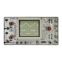
ADJUSTMENT PROCEDURE
If the 492/492P operation is out of tolerance for a par
ticular specification, determine the cause, repair if neces
sary, then use the appropriate adjustment procedure to
return the instrument operation to specification. After any
adjustment, repeat that part of the Performance Check to
verify operation.
Allow instrument to warm up for at least two hours in
ambient air of +20°C to +30°C before performing an
adjustment.
Waveform illustrations used in these instructions may be
idealized. They are not intended to be representative of
specification tolerances.
Adjustment steps that interact are noted, and reference
is made within the procedure to the affected circuit or steps.
STATIC DISCHARGE CAN DAMAGE MANY
SEMICONDUCTOR COMPONENTS USED IN THIS
INSTRUMENT.
Many semiconductor components, especially MOS
types, can be damaged by static discharge. Damage
may not be catastrophic, therefore, not immediately
apparent. It usually appears as a ‘weakening’ of the
semiconductor characteristics. Devices that are par
ticularly susceptible are: MOS, CMOS, JFETs, and
high impedance operational amplifiers. Damage can
be significantly reduced by observing the following
precautions.
1. Handle static-sensitive components or circuit
assemblies at or on a static-free surface. Work station
areas should contain a static-free bench cover or
work plane such as conductive polyethylene sheeting
and a grounding wrist strap. The work plane should
be connected to earth ground.
2. All test equipment, accessories, and soldering
tools should be connected to earth ground.
3. Minimize handling by keeping the components
in their original containers until ready for use. Minimize
the removal and installation of semiconductors from
their circuit boards.
4. Hold the IC devices by their body rather than
the terminals.
5. Use containers made of conductive material or
filled with conductive material for storage and trans
portation. Avoid using ordinary plastic containers. Any
static sensitive part or assembly (circuit board) that is
to be returned to Tektronix, Inc., should be packaged
in its original container or one with anti-static
packaging material.
Table 3-9
ADJUSTMENT STEPS FOR CALIBRATING THE
492/492P
Adjustment Step Page
1. Check and adjust low voltage power supply · ■ ■ 3-43
2. Crt display........................................................ 3-44
3. Deflection amplifier, gain and frequency response 3-45
4. Adjust sweep timing......................................... 3-47
5. Calibrate the 1 st LO system and center frequency
control.............................................................. 3-50
6 . Check 2nd LO frequency and adjust tuning range 3-53
7. Adjust 1 st converter bias
.................................
..
3-57
8 . Baseline leveling (Video Processor)..................
..
3-58
9. Log amplifier calibration...................................
..
3-61
10. Calibrating the resolution bandwidth and shape
factor................................................................ 3-63
11. Presetting the variable resolution gain and band
leveling.............................................................. 3-66
12. Calibrator output level.......................................
..
3-68
13. IF gain calibration.............................................
..
3-68
14. Digital storage calibration
.................................
..
3-69
15. Setting B-SAVE A reference level
..................
..
3-71
16. Band leveling for coaxial bands (1—5)
..............
..
3-71
17. Band leveling for waveguide bands (6 —11).... 3-72
18. Preselector driver (Option 01) calibration
..........
..
3-73
19. Phaselock calibration
.......................................
..
3-76
3-42
REV AUG 1981
 Loading...