•
•
This plOcedure assumes that
you
have performed the Power
Suppy
Primary
t
ro
ubleS
hooting
procedure
WARNING I
Tum the power off. Remove the
jumper from
U4A
pin
6.
This will
remove the low-bulk fault and allow
Line voltage and voltages up
to
800
VDC
are accessible during this
procedure. Refer to the Safety Summary at the front
of
this manual for
S.:;Jfety
informt:Jtion. Turn the
power
switch
off
and
unplug
the
power
curd
before starting this troubleshooting procedure.
the
Main
Convener
to
start
,
Tum
1he power
on.
Us
ing J6 pin 39
as
ground, measure the output
voltage
of
each
supply
listed
in
Table 9-14.
Are
all supplies
at their correct
voltages?
No
Tum the
power
of
. Remove
all
jumpers
and
power sources. Check the power
supply with
normal
line input and loads.
Too
much power is being drawn
Doe,
thevo/lage
at
C12
drop?
Yes
somewhere. Check
and
repair each supply
r:~----I
output
and
its associated components
for
1--------1
shorts. (With both
power
switches
oft
you
should be able
10
charge the
output
of
No
each
supply
wrJ"J
an
external supply.)
I,
>~~--~.r~~~~~~~~~~~---------~~
the
sU'""'"y
Y",
~_
1""1""
...........
k
and
repair "chirp"
rTKXle
in ·chirp·
fault
circuits. (See
Table
9-13
.)
mode?
No
07
and
~receiving
';Y~":...
__
.rCh~OC~k~Ihe~~d~,ru~
·
n~"",,~~g~"~0~I~a:;]7
'-~
_________
...J
gate
we?
(See = and
08
and the
vottage
on
T6.
r
Figure
9-153.)
No
Go to
the
start of this
procechxe and check
for
current limit.
rDS
520
Component
Level Diagnostic and Repair Manual
Scans
by
ArtekMedia =>
2011
CHl
A l}A
:s
;
z.se
u ;U
ER
T
...
.
.....
'
r'
....
"""
..
=~~
.;;:;;
· . .
· . .
· . .
_.-
.
..
--
7
..
--.---
..
--
~
--
...
-
..
--
--
..
~
---
..
. ..
"-
-
'-~
-"
-----.'
-"
""--'
._
.....
..,
...
--
...
-
._
-
....
_-
1
......
~
............. , .................... -
SE'l
j n
ON
I n F F
CHl
r:
OUPl..
I
NG
:
A;C
Or:
G
NO
1
__
-
IN
UE
R T
ON
'OFF
1
__
-
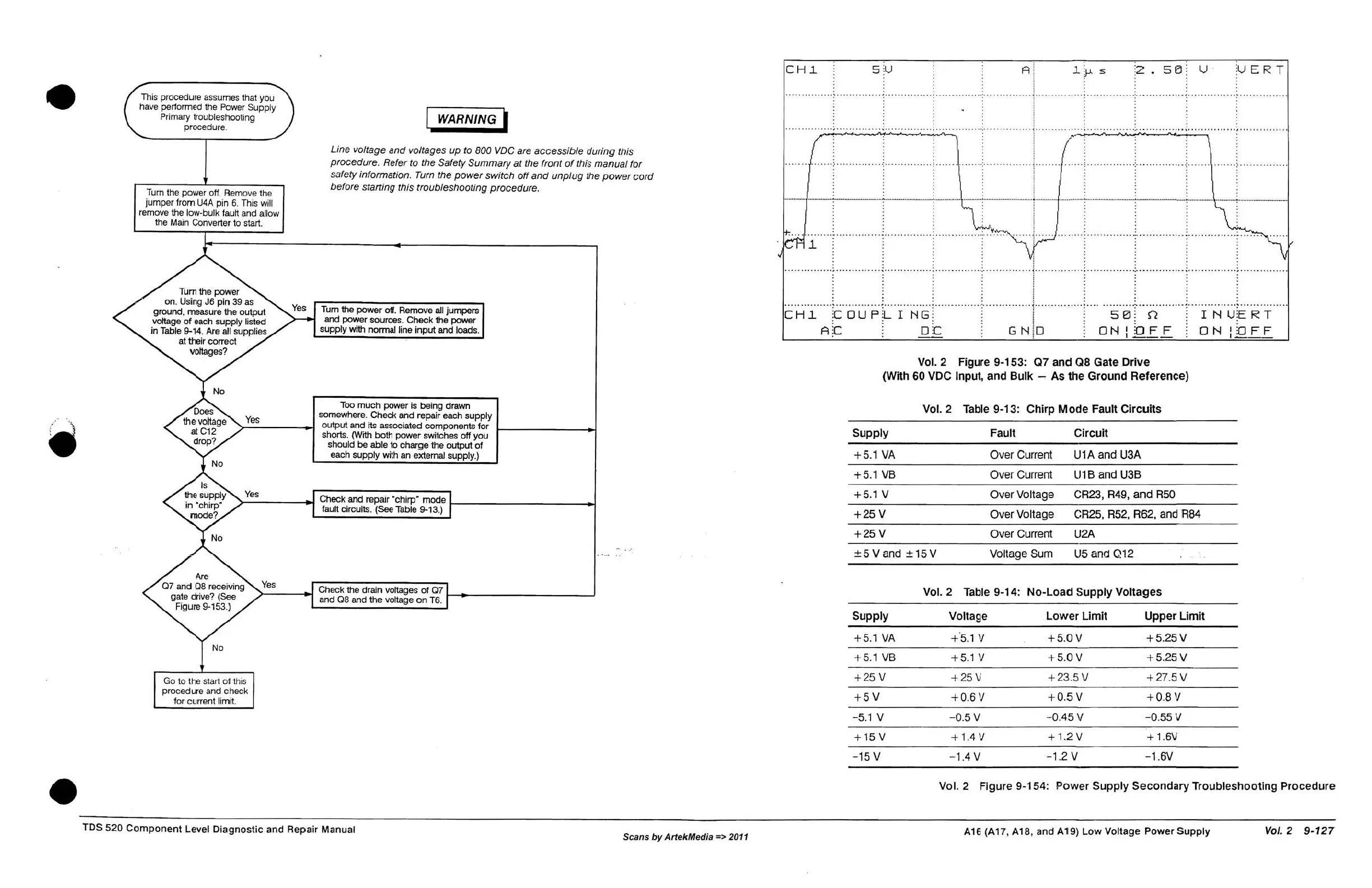
Vol. 2 Figure 9-153: Q7 and
08
Gate Drive
(With 60 VDC Input, and
Bulk
-
As
the Ground Reference)
Vol. 2 Table 9-13: Chirp
Mode
Fault
Circuits
Supply
Fault Circuit
+
5,1
VA
Over Current U1A and U3A
+5.
1
VB
Over Current
U1B
and U3B
+5.1 V Over Voltage CR23, R49,
and
RSO
+25
V Over Voltage
CR25,
R52,
R62, and R84
+25V
Over Current
U2A
±5Vand
±15V
Voltage
Sum
US
and
Q12
Vol. 2 Table 9·14:
No-load
Supply
Voltages
Supply
Voltage
Lower
Limit Upper Limit
+5
.1
VA
+"5.1 V
+5.0'1
+5
.2
5V
+5
.1
VB
+5
.1
V +
5.0V
+ S.2S V
+25
V
+2
5'1
+ 23.5 V +
27.5
V
+
5V
+0.6'1
+ 0.
5V
+ 0.8 V
-5
.1
V - 0.5 V
-0.45 V - 0,
55
V
+ 15 V + 1.4 V
+
1.2V
+ 1.6V
-15 V
-1
.4
V
-1.2
V
-1.6V
Vol. 2 Figure 9·154:
Power
Supply
Secondary
Troubleshooting
Procedure
A16
(A17,
AlB
,
and
A19) L
ow
Vo
ltage Power
Supply
Vol.2
9·127



 To Next Page