5
6
7
8
9
10
INNR
PLIMIT
GVDD
GAIN/SLV
GND
2
1
1
2
C5
1 Fµ
2 1
51 k
R1
51 k
R2
14
TPA3116D2
,
TPA3118D2
,
TPA3130D2
SLOS708G –APRIL 2012–REVISED DECEMBER 2017
www.ti.com
Product Folder Links: TPA3116D2 TPA3118D2 TPA3130D2
Submit Documentation Feedback Copyright © 2012–2017, Texas Instruments Incorporated
Feature Description (continued)
(1) Resistor tolerance should be 5% or better.
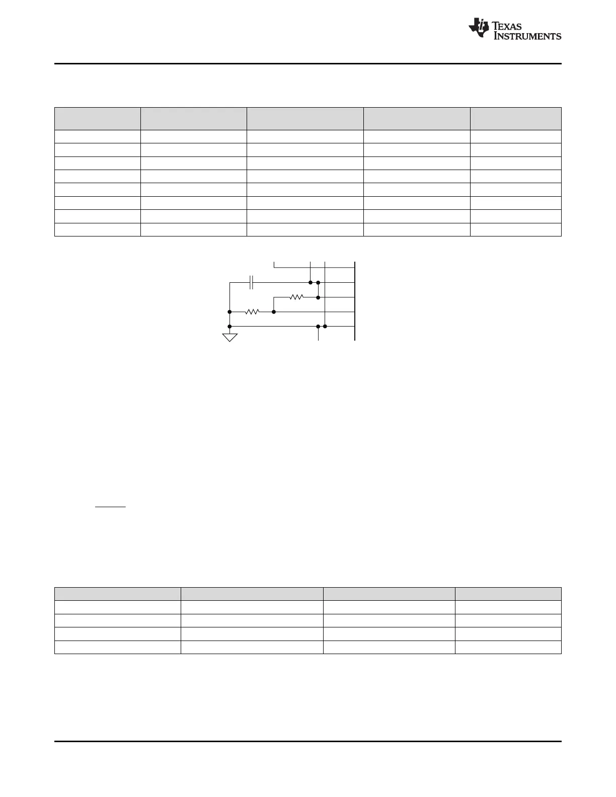
Table 1. Gain and Master/Slave
MASTER / SLAVE
MODE
GAIN R1 (to GND)
(1)
R2 (to GVDD)
(1)
INPUT IMPEDANCE
Master 20 dB 5.6 kΩ OPEN 60 kΩ
Master 26 dB 20 kΩ 100 kΩ 30 kΩ
Master 32 dB 39 kΩ 100 kΩ 15 kΩ
Master 36 dB 47 kΩ 75 kΩ 9 kΩ
Slave 20 dB 51 kΩ 51 kΩ 60 kΩ
Slave 26 dB 75 kΩ 47 kΩ 30 kΩ
Slave 32 dB 100 kΩ 39 kΩ 15 kΩ
Slave 36 dB 100 kΩ 16 kΩ 9 kΩ
Figure 27. Gain, Master/Slave
In Master mode, SYNC terminal is an output, in Slave mode, SYNC terminal is an input for a clock input. TTL
logic levels with compliance to GVDD.
7.3.2 Input Impedance
The TPA31xxD2 family input stage is a fully differential input stage and the input impedance changes with the
gain setting from 9 kΩ at 36 dB gain to 60 kΩ at 20 dB gain. Table 1 lists the values from min to max gain. The
tolerance of the input resistor value is ±20% so the minimum value will be higher than 7.2 kΩ. The inputs need to
be AC-coupled to minimize the output dc-offset and ensure correct ramping of the output voltages during power-
ON and power-OFF. The input ac-coupling capacitor together with the input impedance forms a high-pass filter
with the following cut-off frequency:
(1)
If a flat bass response is required down to 20 Hz the recommended cut-off frequency is a tenth of that, 2 Hz.
Table 2 lists the recommended ac-couplings capacitors for each gain step. If a -3 dB is accepted at 20 Hz 10
times lower capacitors can used – for example, a 1 µF can be used.
Table 2. Recommended Input AC-Coupling Capacitors
GAIN INPUT IMPEDANCE INPUT CAPACITANCE HIGH-PASS FILTER
20 dB 60 kΩ 1.5 µF 1.8 Hz
26 dB 30 kΩ 3.3 µF 1.6 Hz
32 dB 15 kΩ 5.6 µF 1.9 Hz
36 dB 9 kΩ 10 µ F 1.8 Hz
 Loading...