LEA-6 / NEO-6 - Hardware Integration Manual
GPS.G6-HW-09007-A Preliminary Design-in
Page 32 of 62
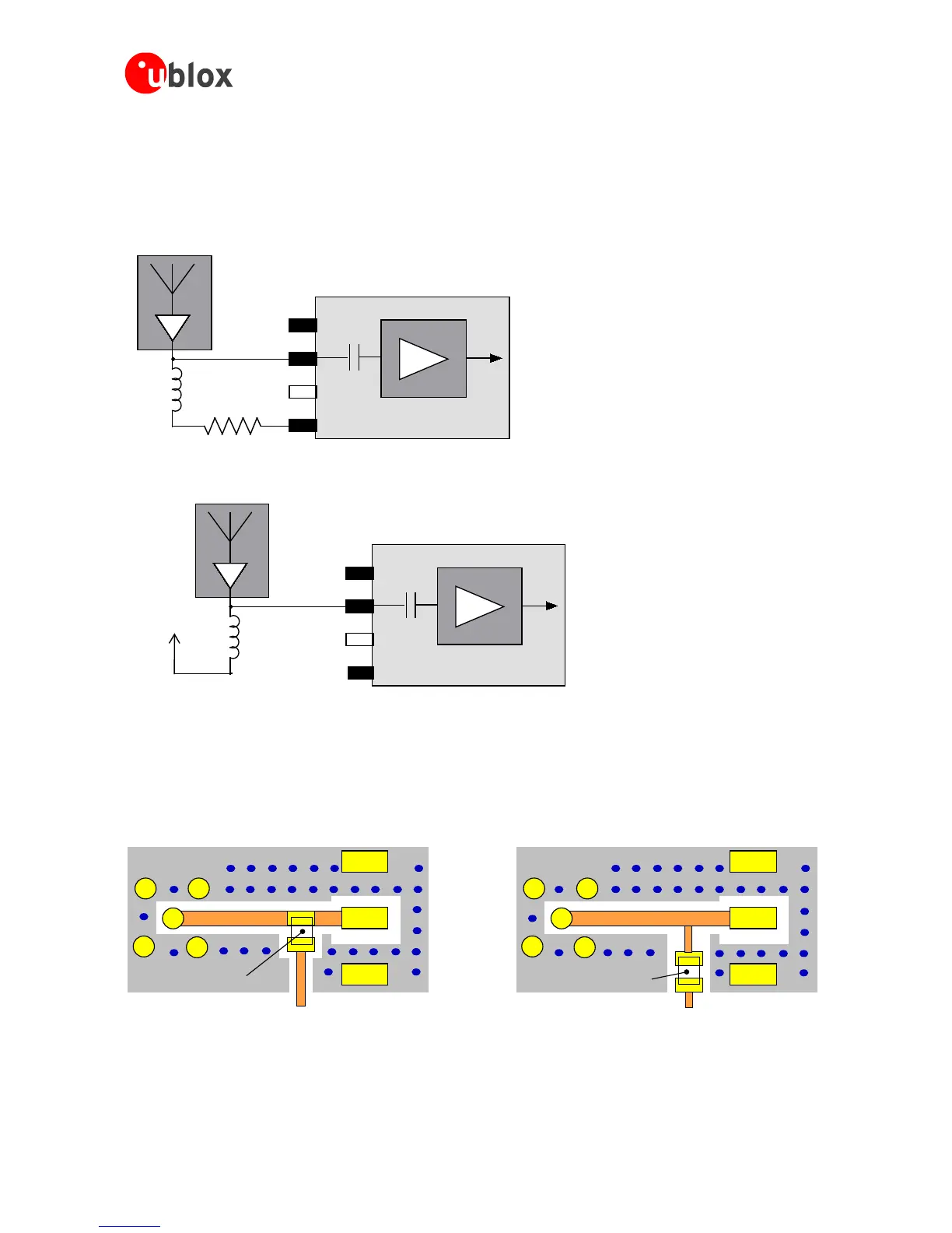
2.5.3 Active antenna (NEO-6)
NEO-6 modules do not provide the antenna bias voltage for active antennas on the RF_IN pin. It is therefore
necessary to provide this voltage outside the module via an inductor as indicated in Figure 25. u-blox
recommends using an inductor from Murata (LQG15HS27NJ02). Alternative parts can be used if the inductor’s
resonant frequency matches the GPS frequency of 1575.4MHz.
Figure 25: Recommended wiring for active antennas (for exact pin orientation see data sheet)
For optimal performance, it is important to place the inductor as close to the microstrip as possible. Figure 24
illustrates the recommended layout and how it should not be done.
 Loading...