SARA-G3 series - System Integration Manual
UBX-13000995 - R06 Objective Specification Design-in
Page 151 of 218
module. If the external signals connected to the wireless module cannot be tri-stated or set low,
insert a multi channel digital switch (e.g. Texas Instruments SN74CB3Q16244, TS5A3159, or
TS5A63157) between the two-circuit connections and set to high impedance during module power
down mode and during the module power-on sequence.
If the GPIO pins are not used, they can be left unconnected on the application board.
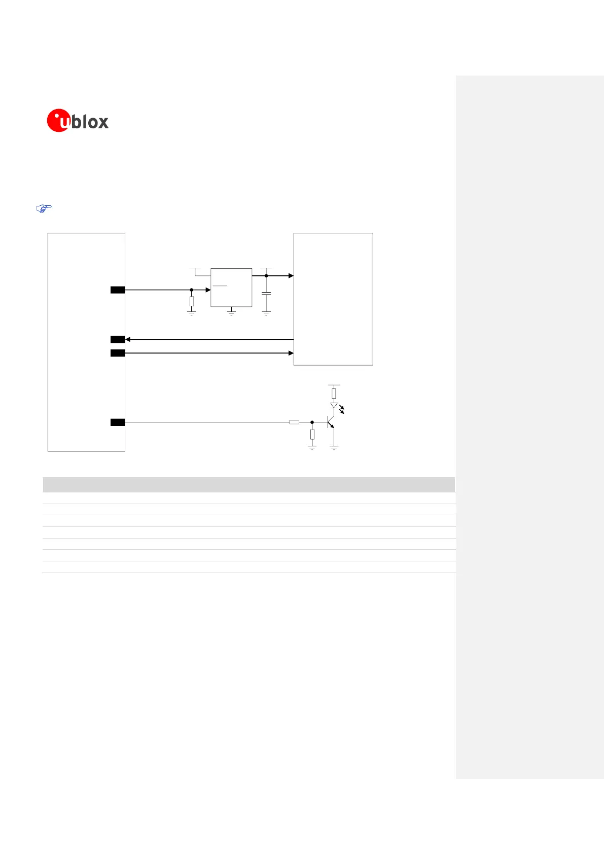
OUTIN
GND
LDO Regulator
SHDN
3V8 1V8
GPIO3
GPIO4
TxD1
EXTINT0
24
25
R1
VCC
GPIO2 23
SARA-G350
u-blox GNSS
1.8 V receiver
U1
C1
R2
R4
3V8
Network Indicator
R3
GNSS Supply Enable
GNSS Data Ready
GNSS RTC Sharing
16
GPIO1
DL1
T1
Figure 61: GPIO application circuit
Part Number - Manufacturer
47 kΩ Resistor 0402 5% 0.1 W
Voltage Regulator for GNSS receiver
See GNSS module Hardware Integration Manual
10 kΩ Resistor 0402 5% 0.1 W
47 kΩ Resistor 0402 5% 0.1 W
820 Ω Resistor 0402 5% 0.1 W
LTST-C190KRKT - Lite-on Technology Corporation
Table 36: Components for GPIO application circuit
2.7.1.1 Guidelines for GPIO layout design
The general purpose input/output pins are generally not critical for layout.
 Loading...