26
J2
11 PA6 Bus to FPGA Counter (Bit 3)
12 PA5 Bus to FPGA Counter (Bit 18)
13 PA4 Bus to FPGA Counter (Bit 4)
14 PA3 Bus to FPGA Counter (Bit 19)
15 PA2 Bus to FPGA Counter (Bit 5)
16 PA1 Bus to FPGA Counter (Bit 20)
17 PC2 Serial communication with USB chip (Rx)
18 PA0 Bus to FPGA Counter (Bit 13)
19 PC0 Coincidence Window or Delay (Bit 1)
20 PC3 Serial communication with USB chip (Tx)
21 PC6_TXA Reserved for firmware upload
22 PC1 Bus to FPGA Counter (Bit 6)
23 PC7_RXA Reserved for firmware upload
24 PG3 Channel Select for FPGA Counter (Bit 0)
25 PG2 Bus to FPGA Counter (Bit 8)
26 PG1 Channel Select for FPGA Counter (Bit 1)
27 PG0 Bus to FPGA Counter (Bit 9)
28 PD0 Clear FPGA Counter Bit
29 PD4 Bus to FPGA Counter (Bit 10)
30 PD5 Enable GATE Signal Flag for FPGA
31 PD6 Bus to FPGA Counter (Bit 11)
32 /RESET_IN Reserved for firmware upload
33 PD7 Bus to FPGA Counter (Bit 12)
34 VBAT_EXT Reserved for Battery Backup
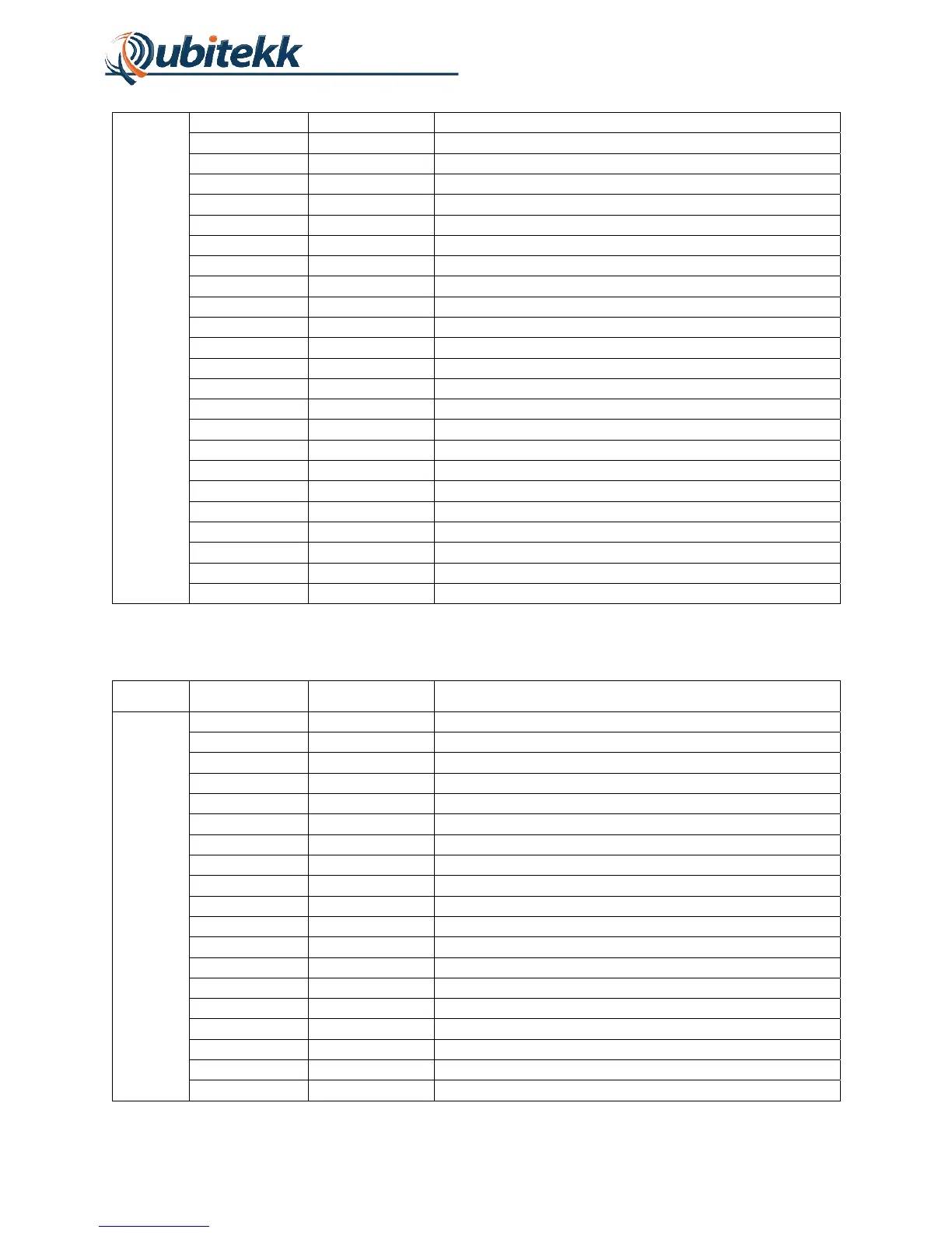
The pinout table for the Cyclone IV FPGA (and DE0-Nano) is as shown below:
Header Pin Number Pin Name Description
JP1
1 IN0 Not Connected
2 IO00 Not Connected
3 IN1 Not Connected
4 IO01 Not Connected
5 IO02 Not Connected
6 IO03 Not Connected
7 IO04 Not Connected
8 IO05 Not Connected
9 IO06 Not Connected
10 IO07 Not Connected
11 +5V +5V Power from USB connector
12 GND Ground
13 IO08 Channel A Signal In
14 IO09 FPGA Counter Output to RCM3400 (Bit 0)
15 IO10 Coincidence Window or Delay (Bit 0)
16 IO11 FPGA Counter Output to RCM3400 (Bit 1)
17 IO12 FPGA Counter Output to RCM3400 (Bit 14)
18 IO13 FPGA Counter Output to RCM3400 (Bit 2)
19 IO14 FPGA Counter Output to RCM3400 (Bit 15)