UM982 User Manual
16 Hardware Design UC-00-M31 EN R1.2
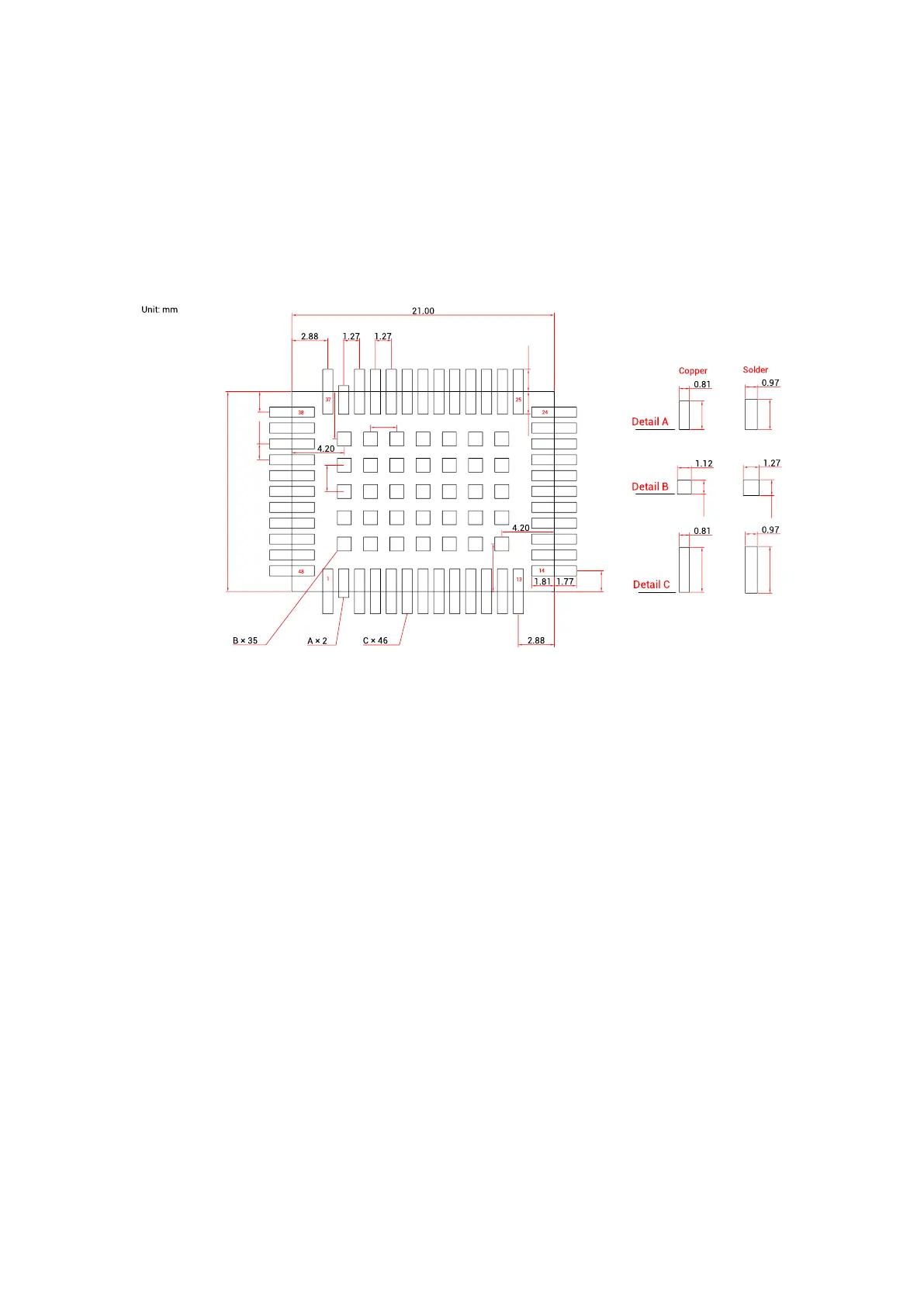
The 35 pads in the rectangle in Figure 3-3 are for grounding and heat dissipation. In the
PCB design, the pads should be connected to a large sized ground to strengthen the
heat dissipation.
3.5 Recommended PCB Package Design
See the following figure for the recommended PCB package design.
Figure 3-4 Recommended PCB Package Design
Notes:
For the convenience of testing, the soldering pads of the pins are designed long,
exceeding the module border much more. For example:
The pads denoted as detail C are 1.77 mm longer than the module border.
The pad denoted as detail A is 0.47 mm longer than the module border. It is
relatively short as it is an RF pin pad, so we hope the trace on the surface is as
short as possible to reduce the impact of external interference on the RF signals.