UM982eb User Manual
4 Interfaces UC-08-M31 EN R1.0
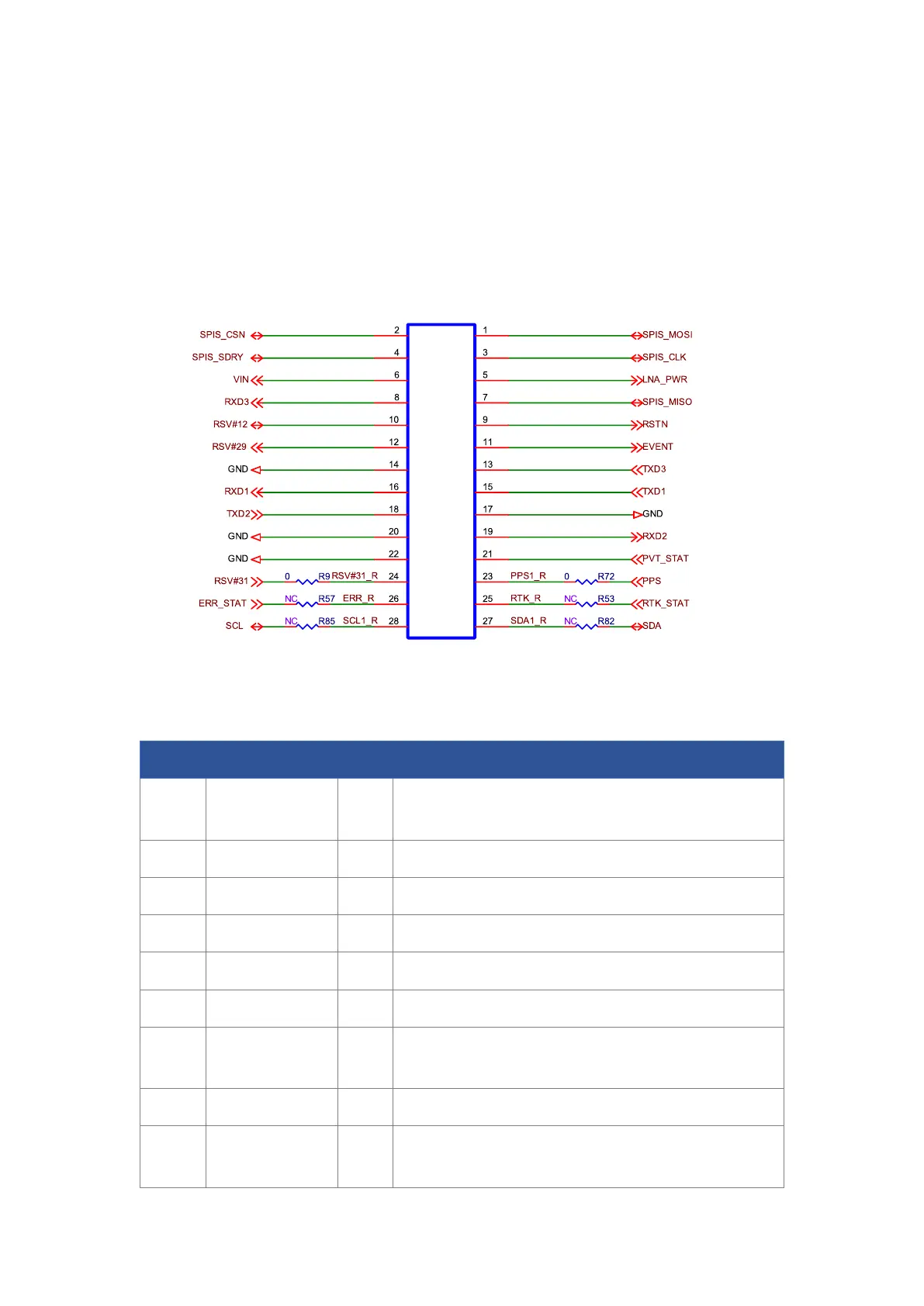
2 Interfaces
The dual-row 28 pins serve as the external interfaces of UM982eb, and the pin pitch is 2
mm. The interfaces can be directly connected to the J18 on Unicore HPL EVK-V5.0 board.
Figure 2-1 UM982eb Interfaces
Table 2-1 UM982eb Pin Description
Master Out / Slave In. This pin is used to receive
data in slave mode.
Chip select pin for SPI slave
Clock input pin for SPI slave
Interrupt output of SPI slave
Antenna feed voltage for LNA
Master In / Slave Out. This pin is used to transmit
data in slave mode.
COM3 input, can be used as CAN RXD, LVTTL
System reset, active low, and the active time should
be no less than 5 ms.