3.2.7
Sync
Amplifier
The
inverted output signal from Hysteresis Switch
Q16
is also
applied to another double
emitter
follower
stage
consisting of
Q19 and Q20. The
output at the common
emitters
of this stage is applied directly
to
the
SYNC OUT
connector
at
the front panel.
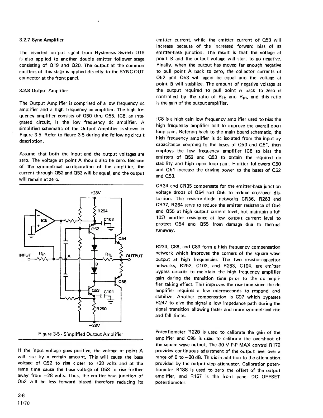
3.2.8
Output Amplifier
The Output Amplifier is comprised
of a low frequency dc
amplifier
and a
high
frequency
ac
amplifier.
The high fre-
quency amplifier consists of 050 thru Q55.
ICS, an inte-
grated circuit, is the low frequency
dc amplifier.
A
simplified
schematic
of
the
Output Amplifier is shown
in
Figure
3-5.
Refer to figure
3-5
during the following
circuit
description.
Assume that both the input
and the
output voltages are
zero.
The voltage
at point A
should
also be zero.
Because
of the
symmetrical configuration
of the amplifier,
the
current through 052 and
053
will
be equal, and
the output
will
remain at zero.
+28V
If the
input
voltage
goes positive, the
voltage at point
A
will
rise by
a certain
amount. This will
cause the
base
voltage
of
Q52
to rise closer
to
-t-28
volts and
at the
same
time
cause the
base voltage of
053 to rise further
away from
—28
volts.
Thus,
the emitter-base
junction of
Q52
will
be less forward
biased
therefore
reducing
its
emitter
current,
while
the emitter current
of 053 will
increase because of the increased forward bias of
its
emitter-base junction. The result is
that the voltage
at
point
B and the output voltage will start to
go
negative.
Finally,
when
the
output has
moved far enough negative
to pull point A back to zero, the
collector currents
of
Q52 and 053 will
again be equal and the voltage
at
point
B
will stabilize. The amount of
negative
voltage at
the
output required to pull point
A
back
to
zero
is
controlled
by
the
ratio of
Rfb
and
Rjn,
and
this
ratio
is
the gain of the
output amplifier.
108 is a high
gain
low
frequency
amplifier used to
bias the
high frequency
amplifier and
to
improve the
overall
open
loop
gain. Refering
back to the
main board
schematic,
the
high
frequency
amplifier
is dc isolated from the
input
by
capacitance
coupling
to the bases of
Q50 and
Q51,
then
employs
the low frequency
amplifier
IC8
to bias the
emitters
of
Q52 and Q53 to obtain
the
required
dc
stability
and
high
open loop
gain. Emitter
followers
Q50
and
Q51
increase the driving
power to the bases
of
Q52
and
Q53.
CR34
and
CR35
compensate for the
emitter-base
junction
voltage
drops of
Q54
and Q55
to reduce crossover
dis-
tortion.
The
resistor-diode
networks
CR36,
R263 and
CR37, R264
serve
to reduce
the emitter
resistance of
Q54
and
Q55 at high
output
current level,
but maintain a full
1012
emitter
resistance
at low
output current
level
to
protect Q54
and
Q55 from
damage due
to
thermal
runaway.
R234,
C88,
and
C89
form
a
high
frequency
compensation
network
which
improves the corners of
the
square wave
output
at
high
frequencies.
The two
resistor-capacitor
networks, R252,
C103,
and R253,
C104, are emitter
bypass
circuits
to maintain
the high
frequency amplifier
gain during the
transition
time prior
to
the
dc ampli-
fier
taking effect.
This improves
the rise
time since
the dc
amplifier
requires
a few
microseconds
to respond and
stabilize.
Another
compensation
is
C97
which
bypasses
R247
to give
the signal
a
low
impedance
path during the
signal transition
allowing faster
and
more symmetrical
rise
and
fall
times.
Potentiometer
R228 is
used to
calibrate
the gain of the
amplifier and
C95 is
used to calibrate
the overshoot
of
the
square wave output. The
30
V P-P
MAX control
R172
provides
continuous
adjustment
of
the output
level over
a
range
of
0 to
—20
dB. This is
in addition
to
the
attenuation
provided
by the output
step
attenuator.
Calibration
poten-
tiometer
R188
is
used to
zero the
offset of
the
output
amplifier,
and
R167
is
the front
panel
DC OFFSET
potentiometer.
3-6
11
.
.'70