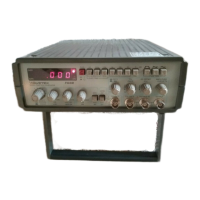
SECTION T
CIRCUIT
DESCRIPTION
This
section
describes the functions
ot majw
circuit
elements
and their
relationships to
one another as
shown in
figure 4-1.
functional Block
digram The
fol-
lowing sections in
this manual
provide more
detailed
information for
maintaining the
instrument
As
shown in
figure
4-1.
the
VCG
(Voltage
Control of
Generator)
sums voltage inputs
from the frequency
dial and
the
VCG IN
connoctor This sum
voltage con-
trots
the magmtudo of
a
complementary current
source and current
sink This current vanes linearity
from approximately 2
mA to
2
|iA over a 1000 1 (4 0
to
004)
range or
logarithmically
from approximately
2
ma to 0 2 »a
over a 10,000 1(4 0 to
0004) range
of
each frequency
multiplier Tho VCG
also controls the
trigger Baseline
compensation circuit,
which consists
of
another current sink at
twice the current
magnitude.
Tho
diode gate,
controlled
By
the
comparator output,
connects
either the current source
or the current sink
to Ihe
timing capacitor
selected
By
the
frequency
multiplier When
the current source is
switched in. the
charge on tho
timing capacitor
will
nse
imeaniy. pro-
ducing the
positive-going
triangle slope. l*ew.se.
the
current sink produces
the negative-go^
triangle
slope.
The triangle
amplifier is a
unity gam amplifier
whose
output is
fed to the
comparator and to the
output cir-
cuits
The comparator
operates
as
a
window detector
with
limit points set to
the triangle peaks
The
tZV
output is
sent Back to the diode gate
and to the
output
circuits.
When the output
is +2V.
the triangle is
positive-gong until
the
+ 1
25V
limit is reached and
the comparator
output switches to -2V
When the
output is
-
2V.
the triangle is
negatrve-gomg
until the
-
1.25V
limit is reached
and the
comparator output
switches
back to * 2V.
repeating the
process in th«s
manner, the basic
function generator
loop, the
Bold
path in figure 4-1.
produces simultaneous
generation
of triangle
and square waves at
the same
frequency
The output
frequency is determined By
the magnitude
of
the timing
capacitor
selected By
tho frequency
multiplier switches and By
the magnitude of the cur-
rents supplied to
and removed from it. Since
the
cur-
rents
are imeanly proportional to the sum ot
the
VCG
inputs,
so
will
Be
the output
frequency.
To extend
the lower frequency
capability
of
the
generator, a
capacitanco multiplier circuit
divides
VCG
currents
By 10
(effectively multiplying
the timing
capacitor
By 10)
tor each of
the lower
3
multiplier
ranges
The TTL squaro from the
comparator is Buftorod and
sent to the SYNC OUT
TTL connector The other side
is sent to
the tnggor flip-flop and to a
level shifter
to
produce the
*2V
bipolar
square for the diodo
gale
and the square shaper circuits
Tho squaro shapor
converts
the
souare
into
a
current signal and applios It
to
the
Tj
FUNCTION
switch
The
Buffered triangle
is
applied
to
the
\
FUNCTION switch
and
to the sino
converter input The sine
convertor, using the
nonlinear characteristics of
its diodes, convorts tho
triangle
into a
sinusoidal current for fhe
%
FUNC-
TION
switch
The selected function is sent to
the preamplifier,
where it is inverted
and Buffered. The preamplifier
out-
put goes to
the
output
amplifier through the
AMPLITUDE
control where it is summed wilh offset
voltage from the
DC
OFFSET control Here, waveform
and offset are inverted and amplified to a ± 10V peak
Signal which can
drive
a 500
termination
from a 500
source 'mpedance
The
output
amplifier drives the
500 OUT HI
connector and
a
resistor divider produc-
ing the
500
OUT
LO
output.
Noncontmuous
modes of operation
(trigger and
gate)
result
from allowing or preventing
the
VCG
current
source from charging the
timing capacitor. Whenever
the trigger tiip-flop output
is low. each
of
the two
trig-
ger diodes conduct a
current
I,
sourcing 21 to
the
baseline
compensation circuit This
removes the cur-
rent I from
the
VCG
current source
and forces
a OV
Baseline at the
triangle amplifier input.
4-1